SBAS677A June   2014  – October 2014 ADS8339

PRODUCTION DATA.  

  1. Features
  2. Applications
  3. Description
  4. Revision History
  5. Device Family
  6. Pin Configuration and Functions
  7. Specifications
    1. 7.1 Absolute Maximum Ratings
    2. 7.2 Handling Ratings
    3. 7.3 Recommended Operating Conditions
    4. 7.4 Thermal Information
    5. 7.5 Electrical Characteristics
    6. 7.6 Timing Requirements
    7. 7.7 Typical Characteristics
  8. Parametric Measurement Information
    1. 8.1 Timing Diagrams
  9. Detailed Description
    1. 9.1 Overview
    2. 9.2 Functional Block Diagram
    3. 9.3 Feature Description
      1. 9.3.1 Analog Input
      2. 9.3.2 Power Saving
      3. 9.3.3 Digital Output
      4. 9.3.4 SCLK Input
    4. 9.4 Device Functional Modes
      1. 9.4.1 CS Mode for a 3-Wire Interface
        1. 9.4.1.1 3-Wire CS Mode Without a Busy Indicator
        2. 9.4.1.2 3-Wire CS Mode With a Busy Indicator
      2. 9.4.2 CS Mode for a 4-Wire Interface
        1. 9.4.2.1 4-Wire CS Mode Without a Busy Indicator
        2. 9.4.2.2 4-Wire CS Mode With a Busy Indicator
      3. 9.4.3 Daisy-Chain Mode
        1. 9.4.3.1 Daisy-Chain Mode Without a Busy Indicator
        2. 9.4.3.2 Daisy-Chain Mode With a Busy Indicator
  10. 10Application and Implementation
    1. 10.1 Application Information
      1. 10.1.1 ADC Reference Driver
        1. 10.1.1.1 Reference Driver Circuit
      2. 10.1.2 ADC Input Driver
        1. 10.1.2.1 Input Amplifier Selection
        2. 10.1.2.2 Antialiasing Filter
    2. 10.2 Typical Application
      1. 10.2.1 Design Requirements
      2. 10.2.2 Detailed Design Procedure
      3. 10.2.3 Application Curve
    3. 10.3 Do's and Don'ts
  11. 11Power-Supply Recommendations
  12. 12Layout
    1. 12.1 Layout Guidelines
    2. 12.2 Layout Example
  13. 13Device and Documentation Support
    1. 13.1 Documentation Support
      1. 13.1.1 Related Documentation
    2. 13.2 Trademarks
    3. 13.3 Electrostatic Discharge Caution
    4. 13.4 Glossary
  14. 14Mechanical, Packaging, and Orderable Information

パッケージ・オプション

メカニカル・データ(パッケージ|ピン)
サーマルパッド・メカニカル・データ
発注情報

8 Parametric Measurement Information

8.1 Timing Diagrams
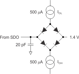
load_cir_digital_iface_bas616.gifFigure 43. Digital Interface Timing Load Circuit
tim_voltage_levels_bas616.gifFigure 44. Timing Voltage Levels