JAJSGS3B January   2019  – July 2022 ADS8353-Q1

PRODUCTION DATA  

  1. 1特長
  2. 2アプリケーション
  3. 3概要
  4. 4Revision History
  5. 5Pin Configuration and Functions
  6. 6Specifications
    1. 6.1 Absolute Maximum Ratings
    2. 6.2 ESD Ratings
    3. 6.3 Thermal Information
    4. 6.4 Recommended Operating Conditions
    5. 6.5 Electrical Characteristics
    6. 6.6 Timing Requirements
    7. 6.7 Switching Characteristics
    8. 6.8 Timing Diagram
    9. 6.9 Typical Characteristics
  7. 7Detailed Description
    1. 7.1 Overview
    2. 7.2 Functional Block Diagram
    3. 7.3 Feature Description
      1. 7.3.1 Reference
      2. 7.3.2 Analog Inputs
        1. 7.3.2.1 Analog Input: Full-Scale Range Selection
        2. 7.3.2.2 Analog Input: Single-Ended and Pseudo-Differential Configurations
      3. 7.3.3 Transfer Function
    4. 7.4 Device Functional Modes
    5. 7.5 Programming
      1. 7.5.1 Serial Interface
      2. 7.5.2 Write to User-Programmable Registers
      3. 7.5.3 Data Read Operation
        1. 7.5.3.1 Reading User-Programmable Registers
        2. 7.5.3.2 Conversion Data Read
          1. 7.5.3.2.1 32-CLK, Dual-SDO Mode (CFR.B11 = 0, CFR.B10 = 0, Default)
          2. 7.5.3.2.2 32-CLK, Single-SDO Mode (CFR.B11 = 0, CFR.B10 = 1)
      4. 7.5.4 Low-Power Modes
        1. 7.5.4.1 STANDBY Mode
        2. 7.5.4.2 Software Power-Down (SPD) Mode
      5. 7.5.5 Frame Abort, Reconversion, or Short-Cycling
    6. 7.6 Register Maps
      1. 7.6.1 ADS8353-Q1 Registers
  8. 8Application and Implementation
    1. 8.1 Application Information
      1. 8.1.1 Input Amplifier Selection
      2. 8.1.2 Charge Kickback Filter
    2. 8.2 Typical Application
      1. 8.2.1 Design Requirements
      2. 8.2.2 Detailed Design Procedure
      3. 8.2.3 Application Curve
    3. 8.3 Power Supply Recommendations
    4. 8.4 Layout
      1. 8.4.1 Layout Guidelines
      2. 8.4.2 Layout Example
  9. 9Device and Documentation Support
    1. 9.1 Device Support
      1. 9.1.1 Development Support
    2. 9.2 Documentation Support
      1. 9.2.1 Related Documentation
    3. 9.3 Receiving Notification of Documentation Updates
    4. 9.4 サポート・リソース
    5. 9.5 Trademarks
    6. 9.6 Electrostatic Discharge Caution
    7. 9.7 Glossary
      1.      Mechanical, Packaging, and Orderable Information

パッケージ・オプション

メカニカル・データ(パッケージ|ピン)
サーマルパッド・メカニカル・データ
発注情報

Analog Input: Single-Ended and Pseudo-Differential Configurations

The ADS8353-Q1 can support single-ended or pseudo-differential input configurations.

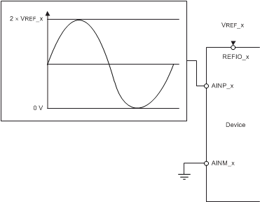
For supporting single-ended inputs, B7 in the configuration register (CFR.B7) must be set to 0 (CFR.B7 = 0) and AINM_A and AINM_B must be externally connected to GND.

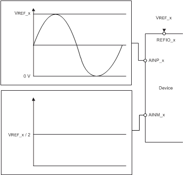
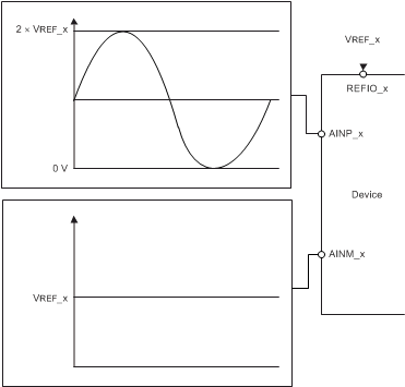
For supporting pseudo-differential inputs, CFR.B7 must be set to 1 (CFR.B7 = 1) and AINM_A and AINM_B must be externally connected to FSR_ADC_A / 2 and FSR_ADC_B / 2, respectively. CFR.B7 is common to both ADCs.

The CFR.B9 and CFR.B7 settings can be combined as shown in Table 7-1 to select the desired input configuration.

Table 7-1 Input Configurations
INPUT RANGE SELECTION AINM SELECTION CONNECTION DIAGRAM
CFR.B9 = 0
(FSR_ADC_A = 0 to VREF_A)
(FSR_ADC_B = 0 to VREF_B)
CFR.B7 = 0
(AINM_A = GND)
(AINM_B = GND)
GUID-9C6632BF-1CF6-4817-9A3D-4889D44E4406-low.gif
CFR.B9 = 1
(FSR_ADC_A = 0 to 2 x VREF_A)
(FSR_ADC_B = 0 to 2 x VREF_B)
CFR.B7 = 0
(AINM_A = GND)
(AINM_B = GND)
GUID-69DD496D-D229-4D47-B994-1A3503764C8B-low.gif
CFR.B9 = 0
(FSR_ADC_A = VREF_A)
(FSR_ADC_B = VREF_B)
CFR.B7 = 1
(AINM_A = VREF_A/2)
(AINM_B = VREF_B/2)
GUID-F90B01C0-4EA0-4C70-B360-304E96E412D3-low.gif
CFR.B9 = 1
(FSR_ADC_A = 2 x VREF_A)
(FSR_ADC_B = 2 x VREF_B)
CFR.B7 = 1
(AINM_A = VREF_A)
(AINM_B = VREF_B)
GUID-4C5BE1E5-40B0-4B17-85E8-6E95AF4B7171-low.gif