SBAS531D December 2010 – February 2016 ADS8555
PRODUCTION DATA.
- 1 Features
- 2 Applications
- 3 Description
- 4 Revision History
- 5 Pin Configuration and Functions
-
6 Specifications
- 6.1 Absolute Maximum Ratings
- 6.2 ESD Ratings
- 6.3 Recommended Operating Conditions
- 6.4 Thermal Information
- 6.5 Electrical Characteristics
- 6.6 Serial Interface Timing Requirements
- 6.7 Parallel Interface Timing Requirements (Read Access)
- 6.8 Parallel Interface Timing Requirements (Write Access)
- 6.9 Typical Characteristics
- 7 Detailed Description
- 8 Applications and Implementation
- 9 Power Supply Recommendations
- 10Layout
- 11Device and Documentation Support
- 12Mechanical, Packaging, and Orderable Information
8 Applications and Implementation
NOTE
Information in the following applications sections is not part of the TI component specification, and TI does not warrant its accuracy or completeness. TI’s customers are responsible for determining suitability of components for their purposes. Customers should validate and test their design implementation to confirm system functionality.
8.1 Application Information
The ADS8555 device enables high-precision measurement of up to six analog signals simultaneously. The following sections summarize some of the typical use cases for the ADS8555 device and the main steps and components used around the analog-to-digital converter.
8.2 Typical Application
8.2.1 Measurement of Electrical Variables in a 3-Phase Power System
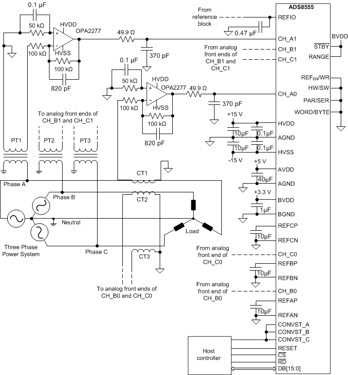
The accurate measurement of electrical variables in a power grid is extremely critical because it helps determine the operating status and running quality of the grid. Such accurate measurements also help diagnose problems with the power network thereby enabling prompt solutions and minimizing down time. The key electrical variables measured in 3-phase power systems are the three line voltages and the three line currents; see Figure 36. These variables enable metrology and power automation systems to determine the amplitude, frequency and phase information to perform harmonic analysis, power factor calculation and power quality assessment among others.
8.2.1.1 Design Requirements
To begin the design process, a few parameters must be decided upon. The designer must know the following:
- Output range of the potential transformers (elements labeled PT1, PT2, and PT3 in Figure 36)
- Output range of the current transformers (elements labeled CT1, CT2, and CT3 in Figure 36)
- Input impedance required from the analog front end for each channel
- Fundamental frequency of the power system
- Number of harmonics that must be acquired
- Type of signal conditioning required from the analog front end for each channel
8.2.1.2 Detailed Design Procedure
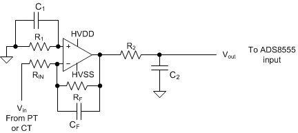
Figure 37 shows the topology chosen to meet the design requirements. A feedback capacitor CF is included to provide a low-pass filter characteristic and attenuate signals outside the band of interest.
 Figure 37. Op Amp in an Inverting Configuration
The potential transformers (PTs) and current transformers (CTs) used in the system depicted in Figure 36 provide the six input variables required. These transformers have a ±10-V output range. Although the PTs and CTs provide isolation from the power system, the value of RIN is selected as 100 kΩ to provide an additional, high-impedance safety element to the input of the ADC. Moreover, selecting a low-frequency gain of –1 V/V (as shown in Equation 5) provides a ±10-V output that can be fed into the ADS8555 device; therefore, the value of RF is selected as 100 kΩ.

The primary goal of the acquisition system depicted in Figure 36 is to measure up to 20 harmonics in a 60-Hz power network. Thus, the analog front-end must have sufficient bandwidth to detect signals up to 1260 Hz, as shown in Equation 6.

Based on the bandwidth found in Equation 6 the ADS8555 device is set to simultaneously sample all six channels at 15.36 kSPS, which provides enough samples to clearly resolve even the highest harmonic required.
The passband of the configuration shown in Figure 37 is determined by the –3-dB frequency according to Equation 7. The value of CF is selected as 820 pF, which is a standard capacitance value available in 0603 size (surface-mount component) and such values, combined with that of RF, result in sufficient bandwidth to accommodate the required 20 harmonics (at 60 Hz).

The value of R1 is selected as the parallel combination of RIN and RF to prevent the input bias current of the operational amplifier from generating an offset error.
The value of component C1 is chosen as 0.1 µF to provide a low-impedance path for noise signals that can be picked up by R1; the 0.1-µF capacitance value improves the EMI robustness and noise performance of the system.
The OPA2277 device is chosen for its low input offset voltage, low drift, bipolar swing, sufficient gain-bandwidth product and low quiescent current. For additional information on the procedure to select SAR ADC input drivers, see reference guide TIDU181.
The charge injection damping circuit is composed of R2 (49.9 Ω) and C2 (370 pF); these components reject high-frequency noise and meet the settling requirements of the ADS8555 device input.
Figure 38 shows the reference block used in this design.
 Figure 38. Op Amp in an Inverting Configuration
For more information on the design of charge injection damping circuits and reference driving circuits for SAR ADCs, consult reference guide TIDU014.
8.2.1.3 Application Curve
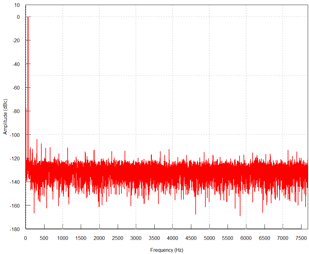
Figure 39 shows the frequency spectrum of the data acquired by the ADS8555 device for a sinusoidal, 20-VPP input at 60 Hz.
 Figure 39. Frequency Spectrum for a Sinusoidal 20-VPP Signal at 60 Hz
The ac performance parameters are:
- SNR: 91.9 dB
- THD: –99.68 dB
- SNDR: 91.23 dB
- SFDR: 103.65 dB
