JAJSDX4 September 2017 ADS8598S
PRODUCTION DATA.
- 1 特長
- 2 アプリケーション
- 3 概要
- 4 改訂履歴
- 5 Pin Configuration and Functions
-
6 Specifications
- 6.1 Absolute Maximum Ratings
- 6.2 ESD Ratings
- 6.3 Recommended Operating Conditions
- 6.4 Thermal Information
- 6.5 Electrical Characteristics
- 6.6 Timing Requirements: CONVST Control
- 6.7 Timing Requirements: Data Read Operation
- 6.8 Timing Requirements: Parallel Data Read Operation, CS and RD Tied Together
- 6.9 Timing Requirements: Parallel Data Read Operation, CS and RD Separate
- 6.10 Timing Requirements: Serial Data Read Operation
- 6.11 Timing Requirements: Byte Mode Data Read Operation
- 6.12 Timing Requirements: Oversampling Mode
- 6.13 Timing Requirements: Exit Standby Mode
- 6.14 Timing Requirements: Exit Shutdown Mode
- 6.15 Switching Characteristics: CONVST Control
- 6.16 Switching Characteristics: Parallel Data Read Operation, CS and RD Tied Together
- 6.17 Switching Characteristics: Parallel Data Read Operation, CS and RD Separate
- 6.18 Switching Characteristics: Serial Data Read Operation
- 6.19 Switching Characteristics: Byte Mode Data Read Operation
- 6.20 Typical Characteristics
-
7 Detailed Description
- 7.1 Overview
- 7.2 Functional Block Diagram
- 7.3 Feature Description
- 7.4
Device Functional Modes
- 7.4.1
Device Interface: Pin Description
- 7.4.1.1 REFSEL (Input)
- 7.4.1.2 RANGE (Input)
- 7.4.1.3 STBY (Input)
- 7.4.1.4 PAR/SER/BYTE SEL (Input)
- 7.4.1.5 CONVSTA, CONVSTB (Input)
- 7.4.1.6 RESET (Input)
- 7.4.1.7 RD/SCLK (Input)
- 7.4.1.8 CS (Input)
- 7.4.1.9 OS[2:0]
- 7.4.1.10 BUSY (Output)
- 7.4.1.11 FRSTDATA (Output)
- 7.4.1.12 DB15/BYTE SEL
- 7.4.1.13 DB14/HBEN
- 7.4.1.14 DB[13:9]
- 7.4.1.15 DB8/DOUTB
- 7.4.1.16 DB7/DOUTA
- 7.4.1.17 DB[6:0]
- 7.4.2 Device Modes of Operation
- 7.4.1
Device Interface: Pin Description
- 8 Application and Implementation
- 9 Power Supply Recommendations
- 10Layout
- 11デバイスおよびドキュメントのサポート
- 12メカニカル、パッケージ、および注文情報
7 Detailed Description
7.1 Overview
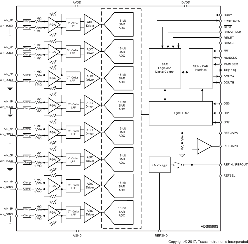
The ADS8598S is an 18-bit data acquisition (DAQ) system with 8-channel analog inputs. Each analog input channel consists of an input clamp protection circuit, a programmable gain amplifier (PGA), a third-order, low-pass filter, and a track-and-hold circuit that facilitates simultaneous sampling of the signals on all input channels. The sampled signal is digitized using an 18-bit analog-to-digital converter (ADC), based on the successive approximation register (SAR) architecture. This overall system can achieve a maximum throughput of 200 kSPS for each channel. The device features a 2.5-V internal reference with a fast-settling buffer, a programmable digital averaging filter to improve noise performance, and high speed serial and parallel interfaces for communication with a wide variety of digital hosts.
The device operates from a single 5-V analog supply and can accommodate true bipolar input signals of ±10 V and ±5 V. The input clamp protection circuitry can tolerate voltages up to ±15 V. The device offers a constant
1-MΩ resistive input impedance irrespective of the sampling frequency or the selected input range. The integration of multiple, simultaneously sampling precision ADC inputs and analog front-end circuits with high input impedance operating from a single 5-V supply offers a simplified end solution without requiring external high-voltage bipolar supplies and complicated driver circuits.
7.2 Functional Block Diagram
7.3 Feature Description
7.3.1 Analog Inputs
The ADS8598S has 8 analog input channels, such that the positive inputs AIN_nP (n = 1 to 8) are the single-ended analog inputs and the negative inputs AIN_nGND are tied to GND. Figure 52 shows the simplified circuit schematic for each analog input channel, including the input clamp protection circuit, PGA, low-pass filter, high-speed ADC driver, and a precision 18-bit SAR ADC.
 Figure 52. Front-End Circuit Schematic for Each Analog Input Channel
The device can support two bipolar, single-ended input voltage ranges based on the logic level of the RANGE input pin. As explained in the RANGE (Input) section, the input voltage range for all analog channels can be configured to bipolar ±10 V or ±5 V. The device samples the voltage difference (AIN_nP – AIN_nGND) between the selected analog input channel and the AIN_nGND pin. The device allows a ±0.3-V range on the AIN_nGND pin for all analog input channels. Use this feature in modular systems where the sensor or signal conditioning block is further away from the ADC on the board and when a difference in the ground potential of the sensor or signal conditioner from the ADC ground is possible. In such cases, running separate wires from the AIN_nGND pin of the device to the sensor or signal conditioning ground is recommended.
7.3.2 Analog Input Impedance
Each analog input channel in the device presents a constant resistive impedance of 1 MΩ. The input impedance for each channel is independent of either the input signal frequency, the configured range of the ADC, or the oversampling mode. The primary advantage of such high-impedance inputs is the ease of driving the ADC inputs without requiring driving amplifiers with low output impedance. Bipolar, high-voltage power supplies are not required in the system because this ADC does not require any high-voltage, front-end drivers. In most applications, the signal sources or sensor outputs can be directly connected to the ADC input, thus significantly simplifying the design of the signal chain.
In order to maintain the dc accuracy of the system, matching the external source impedance on the AIN_nP input pin with an equivalent resistance on the AIN_nGND pin is recommended (see Figure 54). This matching helps to cancel any additional offset error contributed by the external resistance.
7.3.3 Input Clamp Protection Circuit
As illustrated in Figure 52, the ADS8598S features an internal clamp protection circuit on each of the 8 analog input channels. Use of external protection circuits is recommended as a secondary protection scheme to protect the device. Using external protection devices helps with protection against surges, electrostatic discharge (ESD), and electrical fast transient (EFT) conditions.
The input clamp protection circuit on the ADS8598S allows each analog input to swing up to a maximum voltage of ±15 V. Beyond an input voltage of ±15 V, the input clamp circuit turns on, still operating off the single 5-V supply. Figure 53 illustrates a typical current versus voltage characteristic curve for the input clamp. There is no current flow in the clamp circuit for input voltages up to ±15 V. Beyond this voltage, the input clamp circuit turns on.
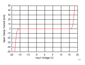 Figure 53. I-V Curve for an Input Clamp Protection Circuit (AVDD = 5 V)
For input voltages above the clamp threshold, make sure that input current never exceeds the absolute maximum rating (see the Absolute Maximum Ratings table) of ±10 mA to prevent any damage to the device. Figure 54 shows that a small series resistor placed in series with the analog inputs is an effective way to limit the input current. In addition to limiting the input current, this resistor can also provide an antialiasing, low-pass filter when coupled with a capacitor. In order to maintain the dc accuracy of the system, matching the external source impedance on the AIN_nP input pin with an equivalent resistance on the AIN_nGND pin is recommended. This matching helps to cancel any additional offset error contributed by the external resistance.
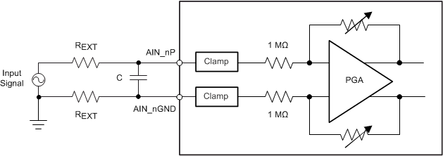 Figure 54. Matching Input Resistors on the Analog Inputs of Device
The input overvoltage protection clamp on the ADS8598S is intended to control transient excursions on the input pins. Leaving the device in a state such that the clamp circuit is activated for extended periods of time in normal or power-down mode is not recommended because this fault condition can degrade device performance and reliability.
7.3.4 Programmable Gain Amplifier (PGA)
The device offers a programmable gain amplifier (PGA) at each individual analog input channel that converts the original single-ended input signal into a fully-differential signal to drive the internal 18-bit SAR ADC. The PGA also adjusts the common-mode level of the input signal before being fed into the ADC to ensure maximum usage of the ADC input dynamic range. Depending on the range of the input signal, the PGA gain can be accordingly adjusted by configuring the RANGE pin of the ADC (see the RANGE (Input) section).
The PGA uses a very highly matched network of resistors for programmable gain configurations. Matching between these resistors and the amplifiers across all channels is accurately trimmed to keep the overall gain error low across all channels and input ranges.
7.3.5 Third-Order, Low-Pass Filter (LPF)
In order to mitigate the noise of the front-end amplifiers and gain resistors of the PGA, each analog input channel of the ADS8598S features a third-order, Butterworth antialiasing, low-pass filter (LPF) at the output of the PGA. Figure 55 and Figure 56 (respectively) show the magnitude and phase response of the analog antialiasing filter. For maximum performance, the –3-dB cutoff frequency for the antialiasing filter is designed to be equal to 24 kHz for the ±10-V range and 16 kHz for the ±5-V range.
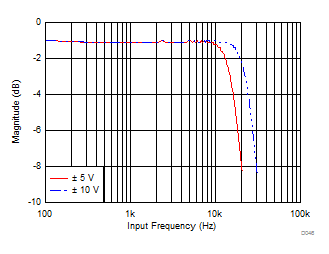 Figure 55. Third-Order LPF Magnitude Response
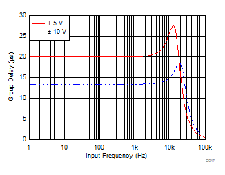 Figure 56. Third-Order LPF Phase Response
7.3.6 ADC Driver
In order to meet the performance of an 18-bit, SAR ADC at the maximum sampling rate (200 kSPS per channel), the capacitors at the input of the ADC must be successfully charged and discharged during the acquisition time window. The inputs of the ADC must settle to better than 18-bit accuracy before any sampled analog voltage gets converted. This drive requirement at the inputs of the ADC necessitates the use of a high-bandwidth, low-noise, and stable amplifier buffer. The ADS8598S features an integrated input driver as part of the signal chain for each analog input. This integrated input driver eliminates the need for any external amplifier, thus simplifying the signal chain design.
7.3.7 Digital Filter and Noise
The ADS8598S features an optional digital averaging filter that can be used in slower throughput applications requiring lower noise and higher dynamic range. As explained in Table 1, the oversampling ratio of the digital filter is determined by the configuration of the OS[2:0] pins. The overall throughput of the ADC decreases proportionally with increase in the oversampling ratio.
Table 1. Oversampling Bit Decoding
| OS[2:0] | OS RATIO | SNR ±10-V INPUT (dB) |
SNR ±5-V INPUT (dB) |
3-dB BANDWIDTH ±10-V INPUT (kHz) |
3-dB BANDWIDTH ±5-V INPUT (kHz) |
MAX THROUGHPUT PER CHANNEL (kSPS) |
|---|---|---|---|---|---|---|
| 000 | No OS | 94.04 | 93.25 | 24 | 16 | 200 |
| 001 | 2 | 95.95 | 94.91 | 23 | 15.7 | 100 |
| 010 | 4 | 96.93 | 95.7 | 19.2 | 14.5 | 50 |
| 011 | 8 | 99.04 | 97.35 | 11.2 | 10.6 | 25 |
| 100 | 16 | 101.41 | 99.03 | 5.6 | 5.6 | 12.5 |
| 101 | 32 | 103.5 | 100.76 | 2.8 | 2.8 | 6.25 |
| 110 | 64 | 104.53 | 101.76 | 1.4 | 1.4 | 3.125 |
| 111 | Invalid | — | — | — | — | — |
In oversampling mode (see the Oversampling Mode of Operation section), the ADC takes the first sample for each channel at the rising edge of the CONVSTA, CONVSTB signals. After converting the first sample, the subsequent samples are taken by an internally generated sampling control signal. The samples are then averaged to reduce the noise of the signal chain as well as to improve the SNR of the ADC. The final output is also decimated to provide a 18-bit output for each channel. Table 1 lists the typical SNR performance for both the ±10-V and ±5-V input ranges, including the –3-dB bandwidth and proportional maximum throughput per channel. When the oversampling ratio increases, there is a proportional improvement in the SNR performance and decrease in the bandwidth of the input filter.
7.3.8 Reference
The ADS8598S can operate with either an internal voltage reference or an external voltage reference using an internal gain amplifier. The internal or external reference selection is determined by an external REFSEL pin, as explained in the REFSEL (Input) section. The REFIN/REFOUT pin outputs the internal band-gap voltage (in internal reference mode) or functions as an input for the external reference voltage (in external reference mode). In both cases, the on-chip amplifier is always enabled. Use this internal amplifier to gain the reference voltage and drive the actual reference input of the internal ADC core for maximizing performance. The REFCAPA (pin 45) and REFCAPB (pin 44) pins must be shorted together externally and a ceramic capacitor of 10 µF (minimum) must be connected between this node and REFGND (pin 43) to ensure that the internal reference buffer is operating as closed loop. Place this capacitor as close as possible to the device to achieve rated performance.
7.3.8.1 Internal Reference
The device has an internal 2.5-V (nominal value) band-gap reference. In order to select the internal reference, the REFSEL pin must be tied high or connected to DVDD. When the internal reference is used, REFIN/REFOUT (pin 42) becomes an output pin with the internal reference value. A 10-μF (minimum) decoupling capacitor, as shown in Figure 57, is recommended to be placed between the REFIN/REFOUT pin and REFGND (pin 43). The capacitor must be placed as close to the REFIN/REFOUT pin as possible. The output impedance of the internal band-gap creates a low-pass filter with this capacitor to band-limit the noise of the band-gap output. The use of a smaller capacitor increases the reference noise in the system, thus degrading SNR and SINAD performance. Do not use the REFIN/REFOUT pin to drive external ac or dc loads because of the limited current output capability of the pin. The REFIN/REFOUT pin can be used as a reference source if followed by a suitable op amp buffer.
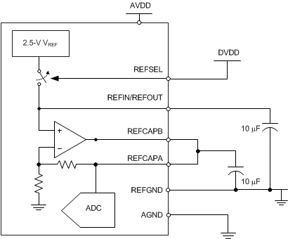 Figure 57. Device Connections for Using an Internal 2.5-V Reference
The device internal reference is factory trimmed to a maximum initial accuracy of ±2.5 mV. The histogram in Figure 58 shows the distribution of the internal voltage reference output taken from more than 2100 devices.
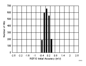 Figure 58. Internal Reference Accuracy at Room Temperature Histogram
The initial accuracy specification for the internal reference can be degraded if the die is exposed to any mechanical, thermal, or environmental stress (such as humidity). Heating the device when being soldered to a printed circuit board (PCB) and any subsequent solder reflow is a primary cause for shifts in the VREF value. The main cause of thermal hysteresis is a change in die stress and therefore is a function of the package, die-attach material, and molding compound, as well as the layout of the device itself.
In order to illustrate this effect, 80 devices were soldered using lead-free solder paste with the suggested manufacturer reflow profile, as explained in the AN-2029 Handling & Process Recommendations application report. The internal voltage reference output is measured before and after the reflow process and Figure 59 shows the typical shift in value. Although all tested units exhibit a positive shift in the output voltages, negative shifts are also possible. The histogram in Figure 59 shows the typical shift for exposure to a single reflow profile. Exposure to multiple reflows, which is common on PCBs with surface-mount components on both sides, causes additional shifts in the output voltage. If the PCB is to be exposed to multiple reflows, solder the ADS8598S in the last pass to minimize device exposure to thermal stress.
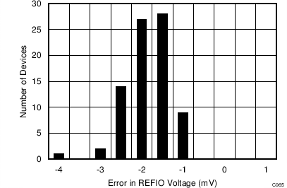 Figure 59. Solder Heat Shift Distribution Histogram
The internal reference is also temperature compensated to provide excellent temperature drift over an extended industrial temperature range of –40°C to +125°C. Figure 60 shows the variation of the internal reference voltage across temperature for different values of the AVDD supply voltage. The typical specified value of the reference voltage drift over temperature is 7.5 ppm/°C.
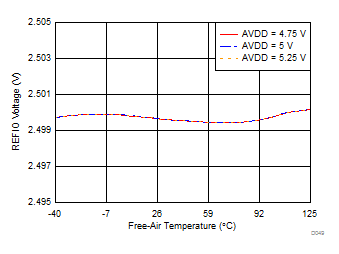 Figure 60. Variation of Internal Reference Output (REFIN/REFOUT) vs Free-Air Temperature and Supply
7.3.8.2 External Reference
For applications that require a reference voltage with lower temperature drift or a common reference voltage for multiple devices, the ADS8598S offers a provision to use an external reference, using the internal buffer to drive the ADC reference pin. In order to select the external reference mode, either tie the REFSEL pin low or connect this pin to AGND. In this mode, an external 2.5-V reference must be applied at REFIN/REFOUT (pin 42), which becomes a high-impedance input pin. Any low-drift, small-size external reference can be used in this mode because the internal buffer is optimally designed to handle the dynamic loading on the ADC reference input. The output of the external reference must be filtered to minimize the resulting effect of the reference noise on system performance. Figure 61 illustrates a typical connection diagram for this mode.
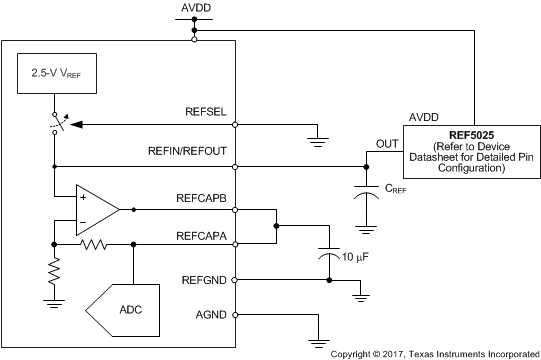 Figure 61. Device Connections for Using an External 2.5-V Reference
For closed-loop operation of the internal reference buffer, the REFCAPA and REFCAPB pins must be externally shorted together. The output of the internal reference buffer appears at the REFCAP pin. A minimum capacitance of 10 µF must be placed between the REFCAPA, REFCAPB pins and REFGND (pin 43). Place this capacitor as close as possible to the REFCAPA and REFCAPB pins. Do not use this internal reference buffer to drive external ac or dc loads because of the limited current output capability.
Figure 62 shows that the performance of the internal buffer output is very stable across the entire operating temperature range of –40°C to +125°C. Figure 63 shows that the typical specified value of the reference buffer drift over temperature is 5 ppm/°C.
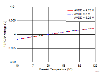 Figure 62. Variation of Reference Buffer Output (REFCAPA, REFCAPB) vs Free-Air Temperature and Supply
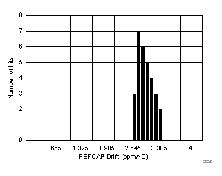
| Number of samples = 30 |
7.3.8.3 Supplying One VREF to Multiple Devices
For applications that require multiple ADS8598S devices, using the same reference voltage source for all ADCs helps eliminate any potential errors in the system resulting from mismatch between multiple reference sources.
Figure 64 illustrates the recommended connection diagram for an application that uses one device in internal reference mode and provides the reference source for other devices. The device used as source of the voltage reference is bypassed by a 10-µF capacitor on the REFIN/REFOUT pin, whereas the other devices are bypassed with a 100-nF capacitor.
 Figure 64. Multiple Devices Connected With an Internal Reference From one Device
Figure 65 shows the recommended connection diagram for an application that uses an external voltage reference (such as the REF5025) to provide the reference source for multiple devices.
 Figure 65. Multiple Devices Connected Using an External Reference
7.3.9 ADC Transfer Function
The ADS8598S is a multichannel device that supports two single-ended, bipolar input ranges of ±10 V and ±5 V on all input channels. The device outputs 18 bits of conversion data in binary two's complement format for both bipolar input ranges. The format for the output codes is the same across all analog channels.
Figure 66 depicts the ideal transfer characteristic for each ADC channel for all input ranges. The full-scale range (FSR) for each input signal is equal to the difference between the positive full-scale (PFS) input voltage and the negative full-scale (NFS) input voltage. The LSB size is equal to FSR / 218 = FSR / 262144 because the resolution of the ADC is 18 bits. Table 2 lists the LSB values corresponding to the different input ranges.
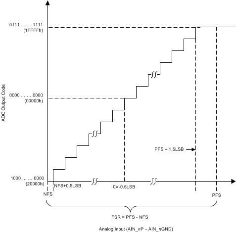 Figure 66. 18-Bit ADC Transfer Function (Two's Complement Binary Format)
Table 2. ADC LSB Values for Different Input Ranges
| INPUT RANGE (V) | POSITIVE FULL-SCALE (V) | NEGATIVE FULL-SCALE (V) | FULL-SCALE RANGE (V) | LSB (µV) |
|---|---|---|---|---|
| ±10 | 10 | –10 | 20 | 76.295 |
| ±5 | 5 | –5 | 10 | 38.1475 |
7.3.10 ADS8598S Device Family Comparison
The ADS8598S belongs to a family of pin-compatible devices. Table 3 lists the devices from this family along with their features.
7.4 Device Functional Modes
7.4.1 Device Interface: Pin Description
7.4.1.1 REFSEL (Input)
The REFSEL pin is a digital input pin that enables selection between the internal and external reference mode of operation for the device. If the REFSEL pin is set to logic high, then the internal reference is enabled and selected. If this pin is set to logic low, then the internal band-gap reference circuit is disabled and powered down. In this mode, an external reference voltage must be provided to the REFIN/REFOUT pin. Under both conditions, the internal reference buffer is always enabled.
The REFSEL pin is an asynchronous logic input. The device output on the REFIN/REFOUT pin starts changing immediately with a change in state of the REFSEL input pin. During power-up, the device wakes up in internal or external reference mode depending on the state of the REFSEL input pin.
7.4.1.2 RANGE (Input)
The RANGE pin is a digital input pin that allows the input range to be selected for all analog input channels. If this pin is set to logic high, the device is configured to operate in the ±10-V input range for all input channels. If this pin is set to logic low, then all input channels operate in the ±5-V input range.
In applications where the input range remains the same for all input channels, the RANGE pin is recommended to be hardwired to the appropriate signal. However, some applications can require an on-the-fly change in the input range by the digital host. For such cases, the RANGE pin functions as an asynchronous input, meaning that any change in the logic input results in an immediate change in the input range configuration of the device. An additional 80 µs must typically be allowed in addition to the device acquisition time for the internal active circuitry to settle to the required accuracy before initiating the next conversion.
The RANGE pin is also used to put the device in standby or shutdown mode depending on the state of the STBY input pin, as explained in the Power-Down Modes section.
7.4.1.3 STBY (Input)
The STBY pin is a digital input pin used to put the device into one of the two power-down modes: standby and shut down. Set the STBY pin to logic high for normal device operation. If this pin is set to logic low, the device enters either standby mode or shutdown mode depending on the state of the RANGE input pin. Both of these modes are low-power modes supported by the device. In shutdown mode, all internal circuitry is powered down, but in standby mode the internal reference and regulators remain powered to enable a relatively quicker recovery to normal operation.
The STBY pin functions as an asynchronous input, meaning that this pin can be pulled low at anytime during device operation to put the device into one of the two power-down modes. However, if the STBY input is set high to bring the device out of power-down mode, then wait for the specified recovery time, as specified in the Timing Requirements: Exit Standby Mode table for proper operation. See the Power-Down Modes section for more details on device operation in the two power-down modes.
7.4.1.4 PAR/SER/BYTE SEL (Input)
The PAR/SER/BYTE SEL pin is a digital input pin that selects between the parallel, serial, or parallel byte interface for reading the data output from the device. If this pin is tied to logic low, then the device operates in the parallel interface mode (see the Parallel Data Read section). If this pin is tied to logic high, then the serial or parallel byte interface mode is selected depending on the state of the DB15/BYTE SEL pin. If the DB15/BYTE SEL is tied low, then serial mode is selected (see the Serial Data Read section) and the parallel byte interface is selected if this pin is tied high (see the Parallel Byte Data Read section).
7.4.1.5 CONVSTA, CONVSTB (Input)
Conversion start A (CONVSTA) and conversion start B (CONVSTB) are active-high, conversion control digital input signals. CONVSTA can be used to simultaneously sample and initiate the conversion process for the first half count of device input channels (channels 1-4), whereas CONVSTB can be used to simultaneously sample and initiate the conversion process for the latter half count of device input channels (channels 5-8). For simultaneous sampling of all input channels, both pins can be shorted together and a single CONVST signal can be used to control the conversion on all input channels. However, in the oversampling mode of operation (see the Oversampling Mode of Operation section), both the CONVSTA and CONVSTB signals must be tied together.
On the rising edge of the CONVSTA, CONVSTB signals, the internal track-and-hold circuits for each analog input channel are placed into hold mode and the sampled input signal is converted using an internal clock. The CONVSTA, CONVSTB signals can be pulled low when the internal conversion is over, as indicated by the BUSY signal (see the BUSY (Output) section). At this point, the front-end circuit for all analog input channels acquire the respective input signals and the internal ADC is not converting. The output data can be read from the device irrespective of the status of the CONVSTA, CONVSTB pins, as there is no degradation in device performance, as explained in the Data Read Operation section.
7.4.1.6 RESET (Input)
The RESET pin is an active-high digital input. A dedicated reset pin allows the device to be reset at any time in an asynchronous manner. All digital circuitry in the device is reset when the RESET pin is set to logic high and this condition remains active until the pin returns low. The device must always be reset after power-up as well as after recovery from shut-down mode when all supplies and references have settled to the required accuracy. If the RESET is issued during an ongoing conversion process, then the device aborts the conversion and output data are invalid. If the reset signal is applied during a data read operation, then the output data registers are all reset to zero.
In order to initiate the next conversion cycle after deactivating a reset condition, allow for a minimum time delay between the falling edge of the RESET input and the rising edge of the CONVSTA, CONVSTB inputs (see the Timing Requirements: CONVST Control table). Any violation in this timing requirement can result in corrupting the results from the next conversion.
7.4.1.7 RD/SCLK (Input)
RD/SCLK is a dual-function pin. Table 4 explains the usage of this pin under different operating conditions of the device.
Table 4. RD/SCLK Pin Functionality
| DEVICE OPERATING CONDITION | FUNCTIONALITY OF THE RD/SCLK INPUT | |
|---|---|---|
| Parallel interface | PAR/SER/BYTE SEL = 0 DB15/BYTE SEL = x |
Functions as an active-low digital input pin to read the output data from the device. In parallel or parallel byte interface mode, the output bus is enabled when both the CS and RD inputs are tied to a logic low input (see the Data Read Operation section). |
| Parallel byte interface | PAR/SER/BYTE SEL = 1 DB15/BYTE SEL = 1 |
|
| Serial interface | PAR/SER/BYTE SEL = 1 DB15/BYTE SEL = 0 |
Functions as an external clock input for the serial data interface. In serial mode, all synchronous accesses to the device are timed with respect to the rising edge of the SCLK signal (see the Serial Data Read section). |
7.4.1.8 CS (Input)
The CS pin indicates an active-low, chip-select signal. A rising edge on the CS signal configures all data lines in tri-state mode. This function allows multiple devices to share the same output data lines. The falling edge of the CS signal marks the beginning of the output data transfer frame in any interface mode of operation for the device. In the parallel and parallel byte interface modes, both the CS and RD input pins must be driven low to enable the digital output bus for reading the conversion data (DB[15:0] for parallel and DB[7:0] for parallel byte interface). In serial mode, the falling edge of the CS signal takes the DOUTA, DOUTB serial data output lines out of tri-state mode and outputs the MSB of the previous conversion result.
7.4.1.9 OS[2:0]
The OS[2:0] pins are active-high digital input pins used to configure the oversampling ratio for the internal digital filter on the device. OS2 is the MSB control bit and OS0 is the LSB control bit. Table 1 provides the decoding of the OS[2:0] bits for different oversampling rates. As described in Table 1, an increase in the OSR mode improves the typical SNR performance for both input ranges and reduces the 3-dB input bandwidth as well as the maximum-allowed throughput per channel.
7.4.1.10 BUSY (Output)
BUSY is an active-high digital output signal. This pin goes to logic high after the rising edges of both the CONVSTA and CONVSTB signals, indicating that the front-end, track-and-hold circuits for all input channels are in hold mode and that the ADC conversion has started. When the BUSY signal goes high, any activity on the CONVSTA or CONVSTB inputs has no effect on the device. The BUSY output remains high until the conversion process for all channels is completed and the conversion data are latched into the output data registers for read out. If the conversion data are read for the previous conversion when BUSY is high, ensure that the data read operation is complete before the falling edge of the BUSY output.
7.4.1.11 FRSTDATA (Output)
FRSTDATA is an active-high digital output signal that indicates if the conversion data output for the first analog input channel of the ADC (AIN_1P and AIN_1GND) is being read out in either of the interface modes. The FRSTDATA output pin comes out of tri-state when the CS input is pulled from a high to a low logic level. Table 5 indicates the functionality of the FRSTDATA output in different interface modes of the device.
Table 5. FRSTDATA Pin Functionality
| DEVICE OPERATING CONDITION | FUNCTIONALITY OF THE FRSTDATA OUTPUT | |
|---|---|---|
| MODE | CONDITIONS | |
| Parallel mode | PAR/SER/BYTE SEL = 0, DB15/BYTE SEL = x |
The first falling edge of the RD signal corresponding to the output result of channel 1 sets the FRSTDATA output to a logic high level. This setting indicates that the data output from channel 1 is being read on the parallel output bus (DB[15:0]). The FRSTDATA output goes low at the third falling edge of the RD signal and remains low until the conversion data output from all other channels is read. |
| Parallel byte mode | PAR/SER/BYTE SEL = 1, DB15/BYTE SEL = 1 |
The first falling edge of the RD signal corresponding to one byte of the output of channel 1 sets the FRSTDATA output to a logic high level. This setting indicates that one byte of the data output from channel 1 is being read on the parallel output bus (DB[7:0]). The FRSTDATA output remains high at the next two falling edges of the RD signal to read the second and third byte of the channel 1 output. This pin goes low on the fourth falling edge of the RD signal and remains low until the conversion data output from all other channels is read. |
| Serial mode | PAR/SER/BYTE SEL = 1, DB15/BYTE SEL = 0 |
The FRSTDATA output goes to a logic high state on the falling edge of the CS signal when the MSB of the channel 1 conversion result is output on DOUTA at this instant. The FRSTDATA pin goes low at the 18th falling edge of the SCLK input, indicating that all 18 bits of the channel 1 output have been read. This pin remains low until the conversion data output from all other channels is read. |
7.4.1.12 DB15/BYTE SEL
DB15/BYTE SEL is a dual-function, digital input, output pin.
When the device operates in parallel interface mode (PAR/SER/BYTE SEL = 0), this pin functions as a digital output. In this mode, this pin is active when the CS signal is pulled low. This pin outputs bit 17 of the conversion result during the first RD pulse and bit 1 of the same conversion result during the second RD pulse.
When the device does not operate in parallel interface mode (PAR/SER/BYTE SEL = 1), this pin functions as a digital control input pin to select between the serial and parallel byte interface modes. The device operates in the serial interface mode when the DB15/BYTE SEL pin is tied low and the device operates in the parallel byte interface mode when this pin is tied to a logic high input.
7.4.1.13 DB14/HBEN
DB14/HBEN is a dual-function, digital input, output pin.
When the device operates in parallel interface mode (PAR/SER/BYTE SEL = 0), this pin functions as a digital output. In this mode, this pin is active when the CS signal is pulled low. This pin outputs bit 16 of the conversion result during the first RD pulse and bit 0 of the same conversion result during the second RD pulse.
When the device operates in parallel byte interface mode (PAR/SER/BYTE SEL = 1 and DB15/BYTE SEL = 1), this pin functions as a digital control input pin that selects if the MSB byte or the LSB byte is output first. If the DB14/HBEN pin is tied to logic high, then the MSB byte (bit[17:10]) is output first followed by the mid byte (bit[9:2]) followed by the LSB byte (bit[1:0] and six zeros) and vice-versa if this pin is tied to logic low.
When the device operates in serial interface mode (PAR/SER/BYTE SEL = 1 and DB15/BYTE SEL = 0), this pin must be tied to AGND or to a logic low input.
7.4.1.14 DB[13:9]
DB[13:9] are digital output pins. In parallel interface mode (PAR/SER/BYTE SEL = 0), these pins output bit 15 to bit 11 of the conversion result for each analog channel when both the CS and RD signals are pulled low. When the device is not in parallel interface mode (PAR/SER/BYTE SEL = 1), these pins must be tied to AGND or to a logic low input.
7.4.1.15 DB8/DOUTB
DB8/DOUTB is a dual-function digital output pin.
In parallel interface mode (PAR/SER/BYTE SEL = 0), use this pin to output bit 10 of the conversion result followed by a zero for each analog channel when both the CS and RD signals are pulled low.
When the device operates in parallel byte interface mode (PAR/SER/BYTE SEL = 1 and DB15/BYTE SEL = 1), this pin remains in a tri-state mode.
In serial interface mode (PAR/SER/BYTE SEL = 1 and DB15/BYTE SEL = 0), this pin outputs the conversion data for the second half count of device input channels (channels 5-8).
7.4.1.16 DB7/DOUTA
DB7/DOUTA is a dual-function digital output pin.
In parallel interface mode (PAR/SER/BYTE SEL = 0), use this pin to output bit 9 of the conversion result followed by a zero for each analog channel when both the CS and RD signals are pulled low.
When the device operates in parallel byte interface mode (PAR/SER/BYTE SEL = 1 and DB15/BYTE SEL = 1), this pin outputs the MSB of the output byte of the conversion data.
In serial interface mode (PAR/SER/BYTE SEL = 1 and DB15/BYTE SEL = 0), use this pin to output conversion data for the first half count of device input channels (channels 1-4).
7.4.1.17 DB[6:0]
DB[6:0] are digital output pins.
In parallel interface mode (PAR/SER/BYTE SEL = 0), these pins output bit 8 to bit 2 of the conversion result followed by a zero for each analog channel when both the CS and RD signals are pulled low.
When the device operates in parallel byte interface mode (PAR/SER/BYTE SEL = 1 and DB15/BYTE SEL = 1), these pins along with the DB7 pin output the 18-bit conversion result in MSB-first fashion in three consecutive RD operations.
When the device operates in serial interface mode (PAR/SER/BYTE SEL = 1 and DB15/BYTE SEL = 0), these pins must be tied to AGND or to a logic low input.
7.4.2 Device Modes of Operation
The ADS8598S supports multiple modes of operation that can be programmed using the hardware pins. This functionality allows the device to be easily configured without any complicated software programming. This section provides details about the normal, power-down (standby and shutdown), and oversampling modes of operation of the device.
7.4.2.1 Power-Down Modes
For applications that are sensitive to power consumption, the ADS8598S offers a built-in, power-down feature. The device supports two power-down modes: standby mode and shutdown mode. As shown in Table 6, the device can enter either power-down mode by pulling the STBY pin to a logic low level. Additionally, the selection between these two power-down modes is done by the state of the RANGE pin.
Table 6. Power-Down Mode Selection
| POWER DOWN MODE | STBY | RANGE |
|---|---|---|
| Standby | 0 | 1 |
| Shutdown | 0 | 0 |
7.4.2.1.1 Standby Mode
The device supports a low-power standby mode in which only part of the circuit is powered down. The analog front-end, signal-conditioning circuit for each channel remains powered down in this mode, but the internal reference and regulator are not powered down. In standby mode, the total power consumption of the device is typically equal to 19 mW.
In order to enter standby mode, the STBY input pin must be set to logic low and the RANGE input pin must be set to a logic high value. The device can be asynchronously put into this mode by configuring the STBY and RANGE inputs at anytime during device operation.
The device exits standby mode when a logic high input is applied to the STBY pin. At this time, the internal circuitry starts powering up and takes a minimum time of 100 µs to settle before the next conversion can be initiated. See the Timing Requirements: Exit Standby Mode table and Figure 8 for timing details.
7.4.2.1.2 Shutdown Mode
The device supports a low-power shutdown mode in which the entire internal circuitry is powered down. In shutdown mode, the total power consumption of the device is typically equal to 1 µW.
In order to enter shutdown mode, the STBY input pin must be set to logic low and the RANGE input pin must be set to a logic low value. The device can be asynchronously put into this mode by configuring the STBY and RANGE inputs at anytime during device operation.
The device exits shutdown mode when a logic high input is applied to the STBY pin. At this time, the internal circuitry starts powering up and takes a minimum time of 13 ms to settle in external reference mode before the next conversion can be initiated. After recovery from shutdown mode, a RESET signal must be applied before the next conversion can be initiated. See the Timing Requirements: Exit Shutdown Mode table and Figure 9 for timing details.
7.4.2.2 Conversion Control
The ADS8598S offers easy and precise control to simultaneously sample all analog input channels or pairs of input channels. The sampling instant can be user-controlled through the digital pins, CONVSTA and CONVSTB. Simultaneously capturing the input signal on all analog input channels is extremely useful in certain applications that are sensitive to additional phase delay between input channels caused by sequential sampling. This section describes the methodology to simultaneously sample all input channels or pairs of input channels for the device.
7.4.2.2.1 Simultaneous Sampling on All Input Channels
The ADS8598S allows all the analog input channels to be simultaneously sampled. In order to do so, the CONVSTA and CONVSTB signals must be tied together (see Figure 67) and a single CONVST signal must be used to control the sampling of all analog input channels of the device. Figure 67 also provides the sequence of events described in this section.
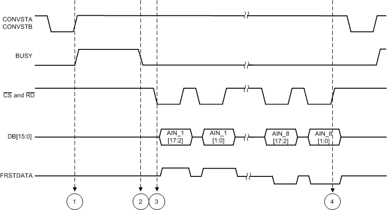 Figure 67. Simultaneous Sampling of All Input Channels in Parallel Interface Timing Diagram
There are four events that describe the internal operation of the device when all input channels are simultaneously sampled and the data are read back. These events are:
- Event 1: Simultaneous sampling of all analog input channels is initiated with the rising edge of the CONVST signal. The input signals on all channels are sampled at this same instant because both the CONVSTA and CONVSTB inputs are tied together. The sampled signals are then converted by the ADC using a precise on-chip oscillator clock. At the beginning of the conversion phase of the ADC, the BUSY output goes high and remains high through a maximum-specified conversion time of tCONV (see the Timing Requirements: CONVST Control table).
- Event 2: At this instant, the ADC has completed the conversion for all input channels and the BUSY output goes to logic low. The falling edge of the BUSY signal indicates the end of conversion and that the internal registers are updated with the conversion data. At this instant, the device is ready to output the correct conversion results for all channels on the parallel output bus (DB[15:0]), or serial output lines (DOUTA, DOUTB), or parallel byte bus (DB[7:0]).
- Event 3: This example shows the data read operation in parallel interface mode with both CS and RD tied together. After BUSY goes low, the first falling edges of CS and RD output the most significant 16 bits conversion result of channel 1 (AIN_1) on the parallel output bus. The next falling edges of CS and RD output the two least significant bits on DB1 and DB0 respectively. Similarly, the conversion results for the remaining channels are output on the parallel bus on subsequent falling edges of the CS and RD signals in a sequential manner. If all channels are not used in the conversion process, tie the unused channels to AGND or any known voltage within the selected input range. The ADC always converts all analog input channels and the results for unused channels are included in the output data stream, thus all unused channels must be tied to AGND or known voltage within the range. The FRSTDATA output goes high on the first falling edges of the CS and RD signals, indicating that the parallel bus is carrying the output result from channel 1. The FRSTDATA output stays high until the AIN_1 data output is read out. On the next falling edges of the CS and RD signals, FRSTDATA goes low and stays low if the CS and RD inputs are low.
- Event 4: After the conversion results for all analog channels are output from the device, the data frame can be terminated by pulling the CS and RD signals to logic high. The parallel bus and FRSTDATA output go to tri-state until the entire sequence is repeated beginning from event 1.
Events 1 and 2 are common to all interface modes of operation (parallel or serial or parallel byte).
7.4.2.2.2 Simultaneous Sampling Two Sets of Input Channels
The ADS8598S allows two sets of analog input channels to be simultaneously sampled. In order to do so, the CONVSTA and CONVSTB signals must be separate control inputs (as shown in Figure 68) and the device must not operate in any oversampling mode. Electrical grid relay protection is an application that can benefit from being able to sample the inputs in two groups. The delay of the signal through the voltage channels is often different from the delay on the channels measuring current. The difference in delay created by the voltage and current signal paths can be corrected by adjusting the sampling of the two groups of inputs (voltage and current) to the device.
The timing diagram of Figure 68 shows the sequence of events described in this section.
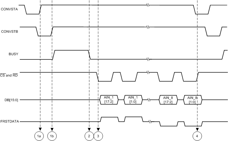 Figure 68. Simultaneous Sampling of All Input Channels in Parallel Interface Timing Diagram
There are four events that describe the internal operation of the device when pairs of input channels are simultaneously sampled and the data are read back. These events are:
- Event 1(a): A rising edge on the CONVSTA signal initiates simultaneous sampling of the first set of analog input channels (channels 1-4). The sampling circuits on the first set of analog input channels enter hold mode and the input signals on these channels are sampled at the same instant. The ADC does not begin conversion until the input signals on the second set of channels are sampled.
- Event 1(b): A rising edge on the CONVSTB signal initiates simultaneous sampling of the second set of analog input channels (channels 5-8). The sampling circuits for the second set of analog input channels enter hold mode and the input signals on these channels are sampled at the same instant. When the rising edges of both the CONVSTA and CONVSTB signals have occurred, the ADC converts all sampled signals using a precise, on-chip oscillator clock. At the beginning of the conversion phase of the ADC, the BUSY output goes high and remains high through a maximum-specified conversion time of tCONV (see the Timing Requirements: CONVST Control table).
- Event 2: Same as event 2 in the Simultaneous Sampling on All Input Channels section.
- Event 3: Same as event 3 in the Simultaneous Sampling on All Input Channels section.
- Event 4: Same as event 4 in the Simultaneous Sampling on All Input Channels section.
Events 1(a), 1(b), and 2 are common to all interface modes of operation (parallel, serial, or parallel byte).
7.4.2.3 Data Read Operation
The ADS8598S updates the internal data registers with the conversion data for all analog channels at the end of every conversion phase (when BUSY goes low). As described in the Timing Requirements: Data Read Operation table, if the output data are read after BUSY goes low, then the device outputs the conversion results for the current sample. However, if the output data are read when BUSY is high, then the device outputs conversion results for the previous sample. Under both conditions, the device supports three interface options as explained in Table 7 depending on the status of the PAR/SER/BYTE SEL and DB15/BYTE SEL pins.
Table 7. Data Read Back Interface Mode Selection
| SELECTED INTERFACE MODE | PAR/SER/BYTE SEL | DB15/BYTE SEL |
|---|---|---|
| Parallel interface | 0 | x |
| Parallel byte interface | 1 | 1 |
| Serial interface | 1 | 0 |
7.4.2.3.1 Parallel Data Read
The ADS8598S supports a parallel interface mode for reading the device output data using the control inputs (CS and RD) the parallel output bus (DB[15:0]), the FRSTDATA indicator, and the BUSY indicator. This interface mode is selected by applying a logic low input on the PAR/SER/BYTE SEL input pin. Depending on the application requirements, the CS and RD control inputs can be tied together or used as separate control inputs in the parallel interface mode.
For applications that use only one device in the system and does not share the parallel output bus with any other devices, the CS and RD input signals can be tied together. Alternatively, the CS signal can be permanently tied low and the RD signal can be used to clock the data out of the device. The timing diagram for this mode of operation is described in the Timing Requirements: Parallel Data Read Operation, CS and RD Tied Together table. In this mode the parallel output bus, DB[15:0], is activated (comes out of tri-state) on the falling edge of the CS/RD signal. At the first falling edge of the CS/RD signal, the most significant 16 bits for output data of channel 1 become available on the parallel bus to be read by the digital host. At the next falling edge of the CS/RD signal, the least significant two bits for output data of channel 1 become available on DB15 and DB14, respectively. The DB[13:0] pins are held low in this pulse. The FRSTDATA output is held high during the data readback of channel 1, indicating channel 1 data are ready to be read back. The output data for the remaining channels are clocked out on the parallel bus on subsequent falling edges of the CS and RD signal in a sequential manner. At the third falling edge of the RD signal, the FRSTDATA output goes low and is held low during this time period when CS and RD are held low.
For applications that use multiple devices in the system, the CS and RD input signals must be driven separately. The timing diagram for this mode of operation is described in the Timing Requirements: Parallel Data Read Operation, CS and RD Separate table. A falling edge of the CS input can be used to activate the parallel bus for a particular device in the system. The RD signal clocks the conversion data out of the device. At the first falling edge of the RD signal, the most significant 16 bits for output data of channel 1 become available on the parallel bus to be read by the digital host. At the next falling edge of the RD signal, the least significant two bits for the output data of channel 1 become available on DB15 and DB14, respectively. The DB[13:0] pins are held low in this pulse. The FRSTDATA output is held high during the data readback of channel 1, indicating channel 1 data are ready to be read back. On subsequent falling edges of the RD signal, the output data for the remaining channels are clocked out on the parallel bus in a sequential manner. At the third falling edge of the RD signal, the FRSTDATA output goes low and remains low until going to tri-state at the next rising edge of the CS signal.
7.4.2.3.2 Parallel Byte Data Read
The ADS8598S supports a parallel byte interface mode for reading the device output data using the control inputs (CS and RD), the parallel output bus (DB[15:0]), the FRSTDATA indicator, and the BUSY indicator. This interface mode is selected by applying a logic high input on the PAR/SER/BYTE SEL input pin and a logic high input on the DB15/BYTE SEL input pin. The parallel byte interface mode is very similar to the parallel interface mode, except that the output data for each channel is read in three data transfers of 8-bit byte sizes.
The order of most significant byte (MSB byte) to least significant byte (LSB byte) is decided by the logic input state of the DB14/HBEN pin. In parallel byte mode, the DB14/HBEN pin functions as a control input. When DB14/HBEN pin is tied high, the MSB byte of the conversion results is output first followed by the Mid byte followed by the LSB byte. This order is reversed when DB14/HBEN is tied to logic low.
The Timing Requirements: Byte Mode Data Read Operation table describes the data read back operation during parallel byte mode when the DB14/HBEN pin is tied high. A falling edge of the CS input is used to activate the parallel bus, DB[7:0] for the device. The RD signal is then used to clock the conversion data out of the device. In this mode, three RD pulses are required to read the full data output for each analog channel. At the first falling edge of the RD signal, the first byte of the channel 1 conversion result becomes available on DB[7:0]. This byte is followed by the second and third bytes of conversion data on the next two falling edges of the RD signal. On subsequent falling edges of the RD signal, the output data for the remaining channels are clocked out in chunks of 8-bit bytes on DB[7:0] in a sequential manner. Thus, a total of 24 RD pulses are required to read the output from all input channels of the ADS8598S.
In this mode, the FRSTDATA output goes high at the first falling edge of the RD signal. FRSTDATA remains high for three RD pulses until channel one conversion result is output. At the fourth falling edge of the RD signal, the FRSTDATA output goes low and remains low throughout the data read operation until going to tri-state at the next rising edge of the CS signal.
The ADC internally appends additional zeros to the 18-bit output data to generate 24-bit data. Table 8 describes the expected output on the three bytes for a given ADC converted code of 34567h for different DB14/HBEN settings.
Table 8. Parallel BYTE Data Read Back
| ADC OUTPUT CODE | DB14/HBEN | 1ST BYTE | 2ND BYTE | 3RD BYTE |
|---|---|---|---|---|
| 34567h | 1 | D1h | 59h | C0h |
| 0 | C0h | 59h | D1h |
7.4.2.3.3 Serial Data Read
The ADS8598S supports a serial interface mode for reading the device output data. This interface mode is selected by applying a logic high input on the PAR/SER/BYTE SEL input pin and a logic low input on the DB15/BYTE SEL input pin. This interface mode uses a CS control input, a communication clock input (SCLK), BUSY and FRSTDATA output indicators, and serial data output lines DOUTA and DOUTB.
Figure 5 illustrates the timing diagram for data read in serial mode for one channel of the ADC, framed by the CS signal. When the CS input is high, the serial data output and FRSTDATA output lines are in tri-state and the SCLK input is ignored. On the falling edge of the CS signal, the output lines become active and the MSB of the conversion result comes out on DOUTA, DOUTB. The MSB can be read by the host processor on the next falling edge of the SCLK signal. The remaining 17 bits of the conversion result are output on the subsequent rising edges of the SCLK signal and can be read by the host processor on the corresponding falling edges. Thus, a total of 18 SCLK cycles are required to clock out 18 bits of conversion result for each channel and the same process can be repeated for the remaining channels in an ascending order. The CS input can be left at a logic low level for the entire data retrieval process for all analog channels or used to frame the retrieval of the 18-bit output data for each analog channel.
The ADS8598S can output the conversion results on one or both of the serial data output lines, DOUTA and DOUTB. The conversion results from the first set of channels (channels 1-4) appear first on DOUTA, followed by the second set of channels (channels 5-8) if only DOUTA is used for reading data. This order is reversed for DOUTB, in which the second set of channels appear first followed by the first set of channels. The use of both data output lines reduces the time needed for data retrieval and a higher throughput can therefore be achieved in this mode.
The FRSTDATA output is in tri-state when the CS signal is high. As illustrated in Figure 5, FRSTDATA goes high on the first falling edge of the CS signal when the MSB of channel 1 is output on DOUTA. The FRSTDATA output remains high for the next 18 SCLK cycles until all data bits of channel 1 are read from the device. The FRSTDATA output returns to a logic low level at the 18th falling edge of the SCLK signal. If data are also read on DOUTB in serial mode, then FRSTDATA remains high when the first channel of the second set of channels is read from the device. The high state of FRSTDATA corresponds to channel 5 for the ADS8598S.
Based on the previous description of the different pins in serial interface mode, conversion data can be read out of the device in several different ways. Some example recommendations are provided below:
- The conversion data can be read out of the device using only one of the two serial output lines, DOUTA or DOUTB. In this case, using DOUTA for output data read back is recommended because channel 1 data appear first on DOUTA followed by the data for other channels in ascending order. To read the data for all channels, provide a total of 18 × 8 = 144 SCLK cycles. This entire data frame can be created within a single CS pulse or each group of 18 SCLK cycles can be individually framed by the CS signal. The primary disadvantage of using just one data line for reading conversion data is that the throughput is reduced if a data read operation is performed after conversion. Figure 69 shows this operation.
- Alternatively, only DOUTB can be used for reading the conversion data from all channels. In this case, everything else remains the same and the output bit stream contains data for all channels in the following order: channels 5, 6, 7, 8, 1, 2, 3, and 4. Figure 69 shows this operation.
- In order to minimize the time for the data read operation in serial mode, both DOUTA and DOUTB can be used to read data out of the device. In this case, the conversion results from the first set of channels (channels 1-4) appear on DOUTA and the conversion results from the second set of channels (channels 5-8) appear first on DOUTB. To read the data for all channels, provide a total of 18 × 4 = 72 SCLK cycles. This entire data frame can be created within a single CS pulse or each group of 18 SCLK cycles can be individually framed by the CS signal. Figure 70 shows this operation.
 Figure 69. Data Read Back in the Serial Interface Using Either DOUTA or DOUTB Timing Diagram
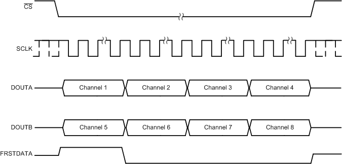 Figure 70. Data Read Back in the Serial Interface Using Both DOUTA and DOUTB Timing Diagram
7.4.2.3.4 Data Read During Conversion
The ADS8598S supports data read operation when the BUSY output is high and the internal ADC is converting. The ADC outputs conversion results for previous sample if data read back is performed during an ongoing conversion. Any of the three interface modes (parallel, parallel byte, or serial) in any combination of oversampling modes can be used to read the device output during an ongoing conversion. The data read back during conversion mode allows faster throughput to be achieved from the device. There is no degradation in performance if data are read from the device during the conversion process, using any of the three interface modes. All channel data must be read before the BUSY signal goes low.
The Timing Requirements: Data Read Operation table describes the timing diagram for data read back during conversion. The timing specification tDZ_CSBSY (the delay between the rising edge of the CS signal and the falling edge of the BUSY signal) must be met because the output data registers are updated with the current conversion results just before the falling edge of the BUSY signal and any read operation during this time can corrupt the register update.
7.4.2.4 Oversampling Mode of Operation
The ADS8598S supports the oversampling mode of operation using an on-chip averaging digital filter, as explained in the Digital Filter and Noise section. The device can be configured in oversampling mode by the OS[2:0] pins (see the OS[2:0] section). Figure 71 shows a typical timing diagram for the oversampling mode of operation. The input on the OS pins is latched on the falling edge of the BUSY signal to configure the oversampling rate for the next conversion.
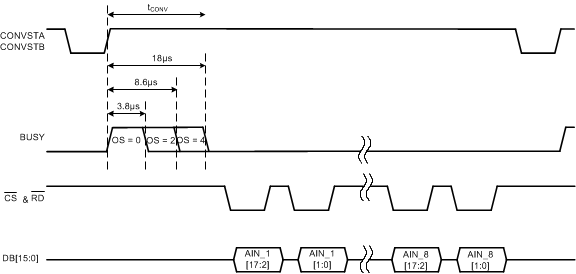 Figure 71. OSR Mode Operation Timing Diagram
In the oversampling mode of operation, both the CONVSTA and CONVSTB signals must be tied together or driven together. As shown in Figure 71, the BUSY signal duration varies with the OSR setting because the conversion time increases with increases in OSR. The high time for the BUSY signal increases with the OSR setting, as listed in the Timing Requirements: CONVST Control table.
For any particular OSR setting, the maximum achievable throughput per channel is specified in Table 1. If the application is running at a lower throughput, then a higher OSR setting can be selected for further noise reduction and SNR improvement. To maximize the throughput per channel, perform a data read when BUSY is high and a conversion is ongoing in OSR mode. This process enables data read for the previous conversion (see the Data Read During Conversion section). At the falling edge of the BUSY signal, the internal data registers are updated with the new conversion data; thus the read operation must complete and CS must be pulled high for at least tDZ_CSBSY before BUSY goes low (see the Timing Requirements: Data Read Operation table).
Oversampling the input signal reduces noise during the conversion process, thus reducing the histogram code spread for a dc input signal to the ADC. Figure 72 to Figure 77 show the effect of oversampling on the output code spread in a dc histogram plot.
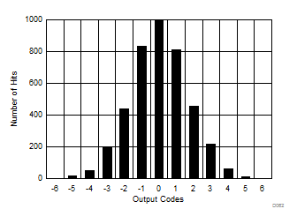
| Mean = 0.03, sigma = 1.52 |
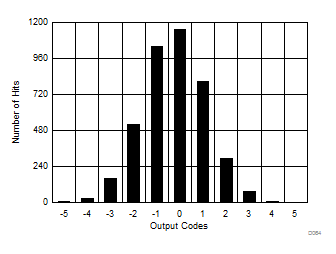
| Mean = –0.25, sigma = 1.09 |
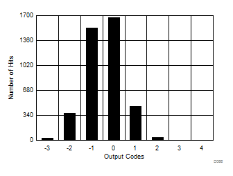
| Mean = –0.44, sigma = 0.75 |
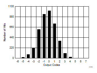
| Mean = –0.33, sigma = 1.39 |
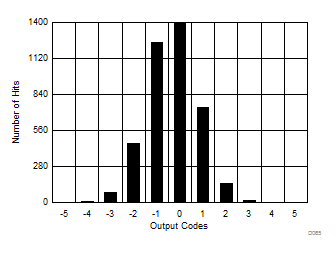
| Mean = –0.33, sigma = 0.89 |
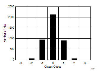
| Mean = –0.02, sigma = 0.72 |
In OSR modes, the device adds a digital filter at the output of the ADC. The digital filter affects the frequency response of the entire data acquisition system including the internal low-pass analog filter and the oversampling digital filter. Figure 78 to Figure 83 show the frequency response curves for different OSR settings in the ±10-V range.
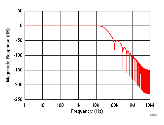
| AVDD = 5 V, DVDD = 5 V, TA = 25°C, input range = ±10 V |
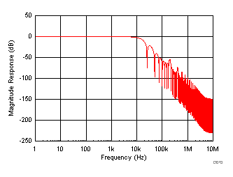
| AVDD = 5 V, DVDD = 5 V, TA = 25°C, input range = ±10 V |
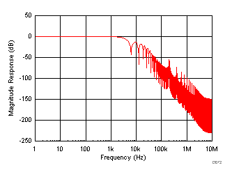
| AVDD = 5 V, DVDD = 5 V, TA = 25°C, input range = ±10 V |
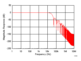
| AVDD = 5 V, DVDD = 5 V, TA = 25°C, input range = ±10 V |
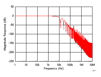
| AVDD = 5 V, DVDD = 5 V, TA = 25°C, input range = ±10 V |
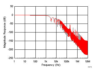
| AVDD = 5 V, DVDD = 5 V, TA = 25°C, input range = ±10 V |