JAJSDX4 September 2017 ADS8598S
PRODUCTION DATA.
- 1 特長
- 2 アプリケーション
- 3 概要
- 4 改訂履歴
- 5 Pin Configuration and Functions
-
6 Specifications
- 6.1 Absolute Maximum Ratings
- 6.2 ESD Ratings
- 6.3 Recommended Operating Conditions
- 6.4 Thermal Information
- 6.5 Electrical Characteristics
- 6.6 Timing Requirements: CONVST Control
- 6.7 Timing Requirements: Data Read Operation
- 6.8 Timing Requirements: Parallel Data Read Operation, CS and RD Tied Together
- 6.9 Timing Requirements: Parallel Data Read Operation, CS and RD Separate
- 6.10 Timing Requirements: Serial Data Read Operation
- 6.11 Timing Requirements: Byte Mode Data Read Operation
- 6.12 Timing Requirements: Oversampling Mode
- 6.13 Timing Requirements: Exit Standby Mode
- 6.14 Timing Requirements: Exit Shutdown Mode
- 6.15 Switching Characteristics: CONVST Control
- 6.16 Switching Characteristics: Parallel Data Read Operation, CS and RD Tied Together
- 6.17 Switching Characteristics: Parallel Data Read Operation, CS and RD Separate
- 6.18 Switching Characteristics: Serial Data Read Operation
- 6.19 Switching Characteristics: Byte Mode Data Read Operation
- 6.20 Typical Characteristics
-
7 Detailed Description
- 7.1 Overview
- 7.2 Functional Block Diagram
- 7.3 Feature Description
- 7.4
Device Functional Modes
- 7.4.1
Device Interface: Pin Description
- 7.4.1.1 REFSEL (Input)
- 7.4.1.2 RANGE (Input)
- 7.4.1.3 STBY (Input)
- 7.4.1.4 PAR/SER/BYTE SEL (Input)
- 7.4.1.5 CONVSTA, CONVSTB (Input)
- 7.4.1.6 RESET (Input)
- 7.4.1.7 RD/SCLK (Input)
- 7.4.1.8 CS (Input)
- 7.4.1.9 OS[2:0]
- 7.4.1.10 BUSY (Output)
- 7.4.1.11 FRSTDATA (Output)
- 7.4.1.12 DB15/BYTE SEL
- 7.4.1.13 DB14/HBEN
- 7.4.1.14 DB[13:9]
- 7.4.1.15 DB8/DOUTB
- 7.4.1.16 DB7/DOUTA
- 7.4.1.17 DB[6:0]
- 7.4.2 Device Modes of Operation
- 7.4.1
Device Interface: Pin Description
- 8 Application and Implementation
- 9 Power Supply Recommendations
- 10Layout
- 11デバイスおよびドキュメントのサポート
- 12メカニカル、パッケージ、および注文情報
8 Application and Implementation
NOTE
Information in the following applications sections is not part of the TI component specification, and TI does not warrant its accuracy or completeness. TI’s customers are responsible for determining suitability of components for their purposes. Customers should validate and test their design implementation to confirm system functionality.
8.1 Application Information
The ADS8598S enables high-precision measurement of up to eight analog signals simultaneously. The device is a fully-integrated data acquisition systems based on an 18-bit successive approximation (SAR) analog-to-digital converter (ADC). The device includes an integrated analog front-end for each input channel and an integrated voltage reference with a precision reference buffer. As such, this device does not require any additional active circuits for driving the analog input pins of the ADC.
8.2 Typical Applications
8.2.1 8-Channel, Data Acquisition System (DAQ) for Power Automation

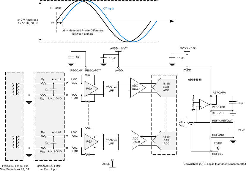
This application example involves the measurement of electrical variables in a power system. The accurate measurement of electrical variables in a power grid is extremely critical because this measurement helps determine the operating status and running quality of the grid. Such accurate measurements also help diagnose potential problems with the power network so that these problems can be resolved quickly without having any significant service impact. The key electrical parameters include amplitude, frequency, and phase measurement of the voltage and current on the power lines. These parameters are important to enable metrology in the power automation system to perform harmonic analysis, power factor calculation, power quality assessment, and so forth.
8.2.1.1 Design Requirements
To begin the design process, a few parameters must be decided upon. The designer must know the following:
- Output range of the potential transformers (elements labeled PT in Figure 84)
- Output range of the current transformers (elements labeled CT in Figure 84)
- Input impedance required from the analog front-end for each channel
- Fundamental frequency of the power system
- Number of harmonics that must be acquired
- Type of signal conditioning required from the analog front-end for each channel
8.2.1.2 Detailed Design Procedure
For the ADS8598S, each channel incorporates an analog front-end composed of a programmable gain amplifier (PGA), analog low-pass filter, and ADC input driver. The analog input for each channel presents a constant resistive impedance of 1 MΩ independent of the ADC sampling frequency and range setting. The high input impedance of the analog front-end circuit allows direct connection to potential transformers (PT) and current transformers (CT). The ADC inputs can support up to ±10-V or ± 5-V bipolar inputs and the integrated signal conditioning eliminates the need for external amplifiers or ADC driver circuits.
The PT and CT used in the system, as illustrated in Figure 84, have a ±10-V output range. Although PT and CT provide isolation from the power system, a series resistor must be placed on the analog input channels. The series resistor helps limit the input current to ±10 mA if the input voltages exceed ±15 V. For applications that require protection against overvoltage or fast transient events beyond the specified absolute maximum ratings of the device, an external protection clamp circuit using transient voltage suppressors (TVS) and ESD diodes is recommended.
A low-pass filter is used on each analog input channel to eliminate high-frequency noise pickup and minimize aliasing. Figure 85 shows an example of the recommended configuration for an input RC filter. A balanced RC filter configuration matches the external source resistance on the positive path (AIN_nP) with an equal resistance on the negative path (AIN_nGND). Matching the source impedance in the positive and negative path allows for better common-mode noise rejection and helps maintain the dc accuracy of the system by canceling any additional offset error contributed by the external series resistance.
 Figure 85. Input RC Low-Pass Filter
The primary goal of the data acquisition system illustrated in Figure 84 is to measure up to 20 harmonics in a 60-Hz power network. Thus, the analog front-end must have sufficient bandwidth (as shown in Equation 1) to detect signals up to 1260 Hz.

Based on the bandwidth calculated in Equation 1, the ADS8598S is set to simultaneously sample all eight channels at 20 kSPS, which is sufficient throughput to clearly resolve the highest harmonic component of the input signal. The pass band of the low-pass filter configuration illustrated in Figure 85 is determined by the –3-dB frequency, calculated according to Equation 2.

The value of CF is selected as 5.6 nF, a standard capacitance value available in 0603-size surface-mount components. In combination with the resistor RF, this low-pass filter provides sufficient bandwidth to accommodate the required 20 harmonics for the input signal of 60 Hz.
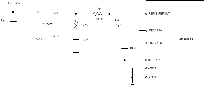
The ADS8598S can operate with either the internal voltage reference or an external reference. The Internal Reference section describes the electrical connections and recommended bypass capacitors when using the internal reference. Alternatively for applications that require a higher precision voltage reference, Figure 86 shows an example of an external reference circuit. The REF5025 provides a very low drift, and very accurate external 2.5-V reference. The resistor RFILT and capacitor CFILT form a low-pass filter to reduce the broadband noise and minimize the resulting effect of the reference noise on the system performance.
 Figure 86. External Reference Circuit for the ADS8598S
8.2.1.3 Application Curve
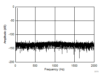
Figure 87 shows the frequency spectrum of the data acquired by the ADS8598S for a sinusoidal, ±10-V input at 60 Hz.
The ac performance parameters measured by this design are:
- SNR = 93.95 dB; SINAD = 93.75 dB
- THD = –105 dB; SFDR = 108.7 dB

8.2.2 Extending the Analog Input Voltage Range
Multiple real-world applications require the ADC to acquire input voltages outside the ±10-V range. This requirement can be achieved by scaling the input signal to match the ADC input voltage range. The existing solutions achieve this matching by using precision-matched resistors to attenuate the signal and buffering the attenuated signal using a suitable amplifier to drive the ADC input. This attenuation needs precision resistors, amplifiers with a required high-voltage supply to buffer the signals. Care must be taken to avoid loading of the source by the attenuator.
 Figure 88. High-Voltage DAQ System
8.2.2.1 Design Requirements
To begin the design process, a few parameters must be decided upon. The designer must know the following:
- Input range of the signal
- Allowed error in the measured output
8.2.2.2 Detailed Design Procedure
For the ADS8598S, each channel incorporates an analog front-end with a constant resistive input impedance of 1 MΩ. The input resistance is independent of the PGA range selection or ADC sampling frequency. The input impedance along with the feedback resistance of the programmable gain amplifier (PGA) help achieve the required attenuation for the input high voltage signal to feed the ADC inputs.
As illustrated in Figure 88, a series resistance can be added to the AIN_nP and AIN_nGND pins. As shown in Equation 3, this series resistance increases the input impedance. When using high values of series resistances, avoid using a parallel capacitor between the AIN_nP and AIN-nGND pins. The leakage current of the capacitor introduces additional gain error.

The increased series resistance along with the PGA feedback resistance increases the attenuation offered by the PGA, thus increasing the allowed input voltage range. Equation 4 calculates the increased input voltage range. Conversely, Equation 5 can be used to calculate the value of series resistance RS based on the required input voltage range.


The additional series resistance introduces gain error in the system because the external resistors have mismatch and are not matched to the internal impedance of the ADC. Thus, high-accuracy, low-drift external resistors must be used. The gain error resulting from mismatch in external resistor and internal resistor must be calibrated to achieve the required accuracy levels.
8.2.2.2.1 Performance Results
Table 9 shows the worst-case accuracy achieved across input range for high-voltage data capture using the design technique described previously at 25°C and 70°C. The RS used for these experiments were chosen to have 0.1% tolerance and temperature drift of 50 ppm/°C.
Table 9. Accuracy With an Extended Input Voltage Range
| ADC RANGE | RS (MΩ) | VIN (Max) | TEMPERATURE | ACCURACY WITHOUT CALIBRATION | ACCURACY WITH CALIBRATION |
|---|---|---|---|---|---|
| ±10 V | 3 | ±40 V | 25°C | 0.726% | 0.003% |
| 70°C | 0.680% | 0.009% | |||
| ±10 V | 1 | ±20 V | 25°C | 0.577% | 0.004% |
| 70°C | 0.502% | 0.003% | |||
| ±10 V | 0.2 | ±12 V | 25°C | 0.205% | 0.001% |
| 70°C | 0.128% | 0.004% | |||
| ±5 V | 3 | ±20 V | 25°C | 0.926% | 0.002% |
| 70°C | 0.753% | 0.006% | |||
| ±5 V | 2 | ±15 V | 25°C | 0.709% | 0.004% |
| 70°C | 0.644% | 0.006% |