JAJSCU6B december   2016  – march 2021 ADS8661 , ADS8665

PRODUCTION DATA  

  1.   1
  2. 特長
  3. アプリケーション
  4. 概要
  5. Revision History
  6. Pin Configuration and Functions
  7. Specifications
    1. 6.1  Absolute Maximum Ratings
    2. 6.2  ESD Ratings
    3. 6.3  Recommended Operating Conditions
    4. 6.4  Thermal Information
    5. 6.5  Electrical Characteristics
    6. 6.6  Timing Requirements: Conversion Cycle
    7. 6.7  Timing Requirements: Asynchronous Reset
    8. 6.8  Timing Requirements: SPI-Compatible Serial Interface
    9. 6.9  Timing Requirements: Source-Synchronous Serial Interface (External Clock)
    10. 6.10 Timing Requirements: Source-Synchronous Serial Interface (Internal Clock)
    11. 6.11 Timing Diagrams
    12. 6.12 Typical Characteristics
  8. Detailed Description
    1. 7.1 Overview
    2. 7.2 Functional Block Diagram
    3. 7.3 Feature Description
      1. 7.3.1 Analog Input Structure
      2. 7.3.2 Analog Input Impedance
      3. 7.3.3 Input Protection Circuit
      4. 7.3.4 Programmable Gain Amplifier (PGA)
      5. 7.3.5 Second-Order, Low-Pass Filter (LPF)
      6. 7.3.6 ADC Driver
      7. 7.3.7 Reference
        1. 7.3.7.1 Internal Reference
        2. 7.3.7.2 External Reference
      8. 7.3.8 ADC Transfer Function
      9. 7.3.9 Alarm Features
        1. 7.3.9.1 Input Alarm
        2. 7.3.9.2 AVDD Alarm
    4. 7.4 Device Functional Modes
      1. 7.4.1 Host-to-Device Connection Topologies
        1. 7.4.1.1 Single Device: All multiSPI Options
        2. 7.4.1.2 Single Device: Standard SPI Interface
        3. 7.4.1.3 Multiple Devices: Daisy-Chain Topology
      2. 7.4.2 Device Operational Modes
        1. 7.4.2.1 RESET State
        2. 7.4.2.2 ACQ State
        3. 7.4.2.3 CONV State
    5. 7.5 Programming
      1. 7.5.1 Data Transfer Frame
      2. 7.5.2 Input Command Word and Register Write Operation
      3. 7.5.3 Output Data Word
      4. 7.5.4 Data Transfer Protocols
        1. 7.5.4.1 Protocols for Configuring the Device
        2. 7.5.4.2 Protocols for Reading From the Device
          1. 7.5.4.2.1 Legacy, SPI-Compatible (SYS-xy-S) Protocols with a Single SDO-x
          2. 7.5.4.2.2 Legacy, SPI-Compatible (SYS-xy-S) Protocols With Dual SDO-x
          3. 7.5.4.2.3 Source-Synchronous (SRC) Protocols
            1. 7.5.4.2.3.1 Output Clock Source Options
            2. 7.5.4.2.3.2 Output Bus Width Options
    6. 7.6 Register Maps
      1. 7.6.1 Device Configuration and Register Maps
        1. 7.6.1.1 DEVICE_ID_REG Register (address = 00h)
        2. 7.6.1.2 RST_PWRCTL_REG Register (address = 04h)
        3. 7.6.1.3 SDI_CTL_REG Register (address = 08h)
        4. 7.6.1.4 SDO_CTL_REG Register (address = 0Ch)
        5. 7.6.1.5 DATAOUT_CTL_REG Register (address = 10h)
        6. 7.6.1.6 RANGE_SEL_REG Register (address = 14h)
        7. 7.6.1.7 ALARM_REG Register (address = 20h)
        8. 7.6.1.8 ALARM_H_TH_REG Register (address = 24h)
        9. 7.6.1.9 ALARM_L_TH_REG Register (address = 28h)
  9. Application and Implementation
    1. 8.1 Application Information
    2. 8.2 Typical Application
      1. 8.2.1 Design Requirements
      2. 8.2.2 Detailed Design Procedure
      3. 8.2.3 Application Curves
  10. Power Supply Recommendations
    1. 9.1 Power Supply Decoupling
    2. 9.2 Power Saving
      1. 9.2.1 NAP Mode
      2. 9.2.2 Power-Down (PD) Mode
  11. 10Layout
    1. 10.1 Layout Guidelines
    2. 10.2 Layout Example
  12. 11Device and Documentation Support
    1. 11.1 Documentation Support
      1. 11.1.1 Related Documentation
    2. 11.2 ドキュメントの更新通知を受け取る方法
    3. 11.3 サポート・リソース
    4. 11.4 Trademarks
    5. 11.5 静電気放電に関する注意事項
    6. 11.6 用語集
  13.   Mechanical, Packaging, and Orderable Information

パッケージ・オプション

メカニカル・データ(パッケージ|ピン)
サーマルパッド・メカニカル・データ
発注情報

Typical Application

GUID-CFFEE36C-ACD8-4CFA-BE90-82A06495B6A9-low.gif
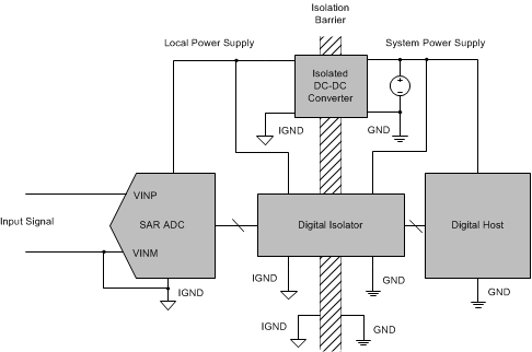
The potential difference between IGND and GND can be as high as the barrier breakdown voltage (often thousands of volts).
Figure 8-1 12-Bit Isolated DAQ System for High Common-Mode Rejection