JAJSCU5B december 2016 – march 2021 ADS8671 , ADS8675
PRODUCTION DATA
- 1
- 1 特長
- 2 アプリケーション
- 3 概要
- 4 Revision History
- 5 Pin Configuration and Functions
-
6 Specifications
- 6.1 Absolute Maximum Ratings
- 6.2 ESD Ratings
- 6.3 Recommended Operating Conditions
- 6.4 Thermal Information
- 6.5 Electrical Characteristics
- 6.6 Timing Requirements: Conversion Cycle
- 6.7 Timing Requirements: Asynchronous Reset
- 6.8 Timing Requirements: SPI-Compatible Serial Interface
- 6.9 Timing Requirements: Source-Synchronous Serial Interface (External Clock)
- 6.10 Timing Requirements: Source-Synchronous Serial Interface (Internal Clock)
- 6.11 Timing Diagrams
- 6.12 Typical Characteristics
-
7 Detailed Description
- 7.1 Overview
- 7.2 Functional Block Diagram
- 7.3 Feature Description
- 7.4 Device Functional Modes
- 7.5 Programming
- 7.6
Register Maps
- 7.6.1
Device Configuration and Register Maps
- 7.6.1.1 DEVICE_ID_REG Register (address = 00h)
- 7.6.1.2 RST_PWRCTL_REG Register (address = 04h)
- 7.6.1.3 SDI_CTL_REG Register (address = 08h)
- 7.6.1.4 SDO_CTL_REG Register (address = 0Ch)
- 7.6.1.5 DATAOUT_CTL_REG Register (address = 10h)
- 7.6.1.6 RANGE_SEL_REG Register (address = 14h)
- 7.6.1.7 ALARM_REG Register (address = 20h)
- 7.6.1.8 ALARM_H_TH_REG Register (address = 24h)
- 7.6.1.9 ALARM_L_TH_REG Register (address = 28h)
- 7.6.1
Device Configuration and Register Maps
- 8 Application and Implementation
- 9 Power Supply Recommendations
- 10Layout
- 11Device and Documentation Support
- Mechanical, Packaging, and Orderable Information
7.5.4.2.2 Legacy, SPI-Compatible (SYS-xy-S) Protocols With Dual SDO-x
The device provides an option to increase the SDO-x bus width from one bit (default, single SDO-x) to two bits (dual SDO-x) when operating with any of the data transfer protocols. In order to operate the device in dual SDO mode, the SDO1_CONFIG[1:0] bits in the SDO_CTL_REG register must be set to 11b. In this mode, the ALARM/SDO-1/GPO pin functions as SDO-1.
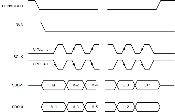
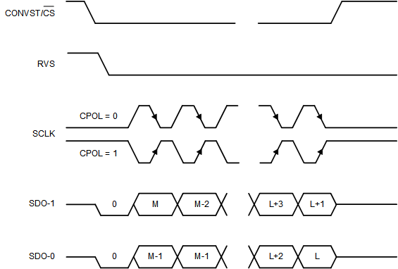
In dual SDO mode, two bits of data are launched on the two SDO-x pins (SDO-0 and SDO-1) on every SCLK launch edge, as shown in Figure 7-30 and Figure 7-31.
 Figure 7-30 Standard SPI Timing Protocol
(CPHA = 0, Dual SDO-x)
 Figure 7-31 Standard SPI Timing Protocol
(CPHA = 1, Dual SDO-x)
For any particular SPI protocol, the device follows the same timing specifications for single and dual SDO modes. The only difference is that the device requires half as many SCLK cycles to output the same number of bits when in single SDO mode, thus reducing the minimum required SCLK frequency for a certain sampling rate of the ADC.