SBAS547D May   2013  – August 2015 ADS8881

PRODUCTION DATA.  

  1. Features
  2. Applications
  3. Description
  4. Revision History
  5. Companion Products
  6. Device Comparison
  7. Pin Configurations and Functions
  8. Specifications
    1. 8.1 Absolute Maximum Ratings
    2. 8.2 ESD Ratings
    3. 8.3 Recommended Operating Conditions
    4. 8.4 Thermal Information
    5. 8.5 Electrical Characteristics
    6. 8.6 Timing Requirements: 3-Wire Operation
    7. 8.7 Timing Requirements: 4-Wire Operation
    8. 8.8 Timing Requirements: Daisy-Chain
    9. 8.9 Typical Characteristics
  9. Parametric Measurement Information
    1. 9.1 Equivalent Circuits
  10. 10Detailed Description
    1. 10.1 Overview
    2. 10.2 Functional Block Diagram
    3. 10.3 Feature Description
      1. 10.3.1 Analog Input
      2. 10.3.2 Reference
      3. 10.3.3 Clock
      4. 10.3.4 ADC Transfer Function
    4. 10.4 Device Functional Modes
      1. 10.4.1 CS Mode
        1. 10.4.1.1 3-Wire CS Mode Without a Busy Indicator
        2. 10.4.1.2 3-Wire CS Mode With a Busy Indicator
        3. 10.4.1.3 4-Wire CS Mode Without a Busy Indicator
        4. 10.4.1.4 4-Wire CS Mode With a Busy Indicator
      2. 10.4.2 Daisy-Chain Mode
        1. 10.4.2.1 Daisy-Chain Mode Without a Busy Indicator
        2. 10.4.2.2 Daisy-Chain Mode With a Busy Indicator
  11. 11Application and Implementation
    1. 11.1 Application Information
      1. 11.1.1 ADC Reference Driver
      2. 11.1.2 ADC Input Driver
        1. 11.1.2.1 Input Amplifier Selection
        2. 11.1.2.2 Antialiasing Filter
    2. 11.2 Typical Applications
      1. 11.2.1 DAQ Circuit for a 1-µs, Full-Scale Step Response
        1. 11.2.1.1 Design Requirements
        2. 11.2.1.2 Detailed Design Procedure
        3. 11.2.1.3 Application Curve
      2. 11.2.2 Low-Power DAQ Circuit for Excellent Dynamic Performance at 1 MSPS
        1. 11.2.2.1 Design Requirements
        2. 11.2.2.2 Detailed Design Procedure
        3. 11.2.2.3 Application Curve
      3. 11.2.3 DAQ Circuit for Lowest Distortion and Noise Performance at 1 MSPS
        1. 11.2.3.1 Design Requirements
        2. 11.2.3.2 Detailed Design Procedure
        3. 11.2.3.3 Application Curve
      4. 11.2.4 Ultralow-Power DAQ Circuit at 10 kSPS
        1. 11.2.4.1 Design Requirements
        2. 11.2.4.2 Detailed Design Procedure
        3. 11.2.4.3 Application Curve
  12. 12Power-Supply Recommendations
    1. 12.1 Power-Supply Decoupling
    2. 12.2 Power Saving
  13. 13Layout
    1. 13.1 Layout Guidelines
    2. 13.2 Layout Example
  14. 14Device and Documentation Support
    1. 14.1 Device Support
      1. 14.1.1 Development Support
    2. 14.2 Documentation Support
      1. 14.2.1 Related Documentation
    3. 14.3 Receiving Notification of Documentation Updates
    4. 14.4 Community Resources
    5. 14.5 Trademarks
    6. 14.6 Electrostatic Discharge Caution
    7. 14.7 Glossary
  15. 15Mechanical, Packaging, and Orderable Information

パッケージ・オプション

メカニカル・データ(パッケージ|ピン)
サーマルパッド・メカニカル・データ
発注情報

12 Power-Supply Recommendations

The device has two separate power supplies: AVDD and DVDD. The internal circuits of the device operate on AVDD; DVDD is used for the digital interface. AVDD and DVDD can be independently set to any value within the permissible range.

12.1 Power-Supply Decoupling

Decouple the AVDD and DVDD pins with GND, using individual 1-µF decoupling capacitors placed in close proximity to the pin, as shown in Figure 74.
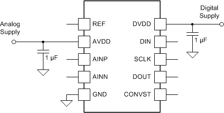
ADS8881 ai_apps_pwr_bas547.gif Figure 74. Supply Decoupling

12.2 Power Saving

The device has an auto power-down feature that powers down the internal circuitry at the end of every conversion. Referring to Figure 75, the input signal is acquired on the sampling capacitors when the device is in a power-down state (tacq); at the same time, the result for the previous conversion is available for reading. The device powers up on the start of the next conversion. During conversion phase (tconv), the device also consumes current from the reference source (connected to the REF pin).
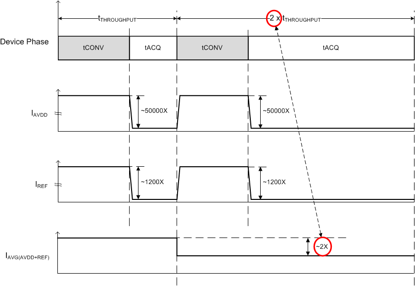
ADS8881 power_scaling_illustration.gif Figure 75. Power Scaling With Throughput

The conversion time, tconv, is independent of the SCLK frequency. When operating the device at speeds lower than the maximum rated throughput, the conversion time, tconv, does not change; the device spends more time in power-down state. Therefore, as shown in Figure 76, the device power consumption from the AVDD supply and the external reference source is directly proportional to the speed of operation. Extremely low AVDD power-down current (50 nA, typical) and extremely low external reference leakage current (250 nA, typical), make this device ideal for very low throughput applications (such as pulsed measurements).
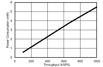
ADS8881 C031_SBAS547.png Figure 76. Power Scaling With Throughput