JAJSCA2B June 2016 – January 2018 ADS8910B , ADS8912B , ADS8914B
PRODUCTION DATA.
- 1 特長
- 2 アプリケーション
- 3 概要
- 4 改訂履歴
- 5 Pin Configuration and Functions
- 6 Specifications
-
7 Detailed Description
- 7.1 Overview
- 7.2 Functional Block Diagram
- 7.3 Feature Description
- 7.4 Device Functional Modes
- 7.5
Programming
- 7.5.1 Output Data Word
- 7.5.2 Data Transfer Frame
- 7.5.3 Interleaving Conversion Cycles and Data Transfer Frames
- 7.5.4 Data Transfer Protocols
- 7.5.5 Device Setup
- 7.6
Register Maps
- 7.6.1
Device Configuration and Register Maps
- 7.6.1.1 PD_CNTL Register (address = 04h) [reset = 00h]
- 7.6.1.2 SDI_CNTL Register (address = 008h) [reset = 00h]
- 7.6.1.3 SDO_CNTL Register (address = 0Ch) [reset = 00h]
- 7.6.1.4 DATA_CNTL Register (address = 010h) [reset = 00h]
- 7.6.1.5 PATN_LSB Register (address = 014h) [reset = 00h]
- 7.6.1.6 PATN_MID Register (address = 015h) [reset = 00h]
- 7.6.1.7 PATN_MSB Register (address = 016h) [reset = 00h]
- 7.6.1.8 OFST_CAL Register (address = 020h) [reset = 00h]
- 7.6.1.9 REF_MRG Register (address = 030h) [reset = 00h]
- 7.6.1
Device Configuration and Register Maps
-
8 Application and Implementation
- 8.1 Application Information
- 8.2 Typical Application
- 9 Power-Supply Recommendations
- 10Layout
- 11デバイスおよびドキュメントのサポート
- 12メカニカル、パッケージ、および注文情報
パッケージ・オプション
メカニカル・データ(パッケージ|ピン)
- RGE|24
サーマルパッド・メカニカル・データ
- RGE|24
発注情報
7.5.4.1 Protocols for Configuring the Device
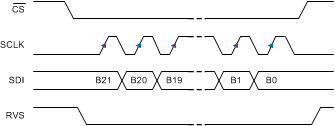
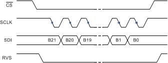
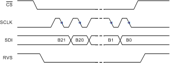
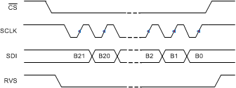
As shown in Table 4, the host controller can use any of the four legacy, SPI-compatible protocols (SPI-00-S, SPI-01-S, SPI-10-S, or SPI-11-S) to write data to the device.
Table 4. SPI Protocols for Configuring the Device
| PROTOCOL | SCLK POLARITY
(At CS Falling Edge) |
SCLK PHASE
(Capture Edge) |
SDI_CNTL | SDO_CNTL | NO. OF SCLK
(Optimal Command Frame) |
TIMING DIAGRAM |
|---|---|---|---|---|---|---|
| SPI-00-S | Low | Rising | 00h | 00h | 22 | Figure 50 |
| SPI-01-S | Low | Falling | 01h | 00h | 22 | Figure 51 |
| SPI-10-S | High | Falling | 02h | 00h | 22 | Figure 52 |
| SPI-11-S | High | Rising | 03h | 00h | 22 | Figure 53 |
At power-up or after coming out of any asynchronous reset, the device supports the SPI-00-S protocol for data-read and data-write operations.
To select a different SPI-compatible protocol, program the SDI_MODE[1:0] bits in the SDI_CNTL register. This first write operation must adhere to the SPI-00-S protocol. Any subsequent data transfer frames must adhere to the newly selected protocol.
Figure 50 to Figure 53 detail the four protocols using an optimal command frame; see the Timing Requirements and Switching Characteristics tables for associated timing parameters.
NOTE
As explained in the Data Transfer Frame section, a valid write operation to the device requires a minimum of 22 SCLKs to be provided within a data transfer frame.
Any data write operation to the device must continue to follow the SPI-compatible protocol selected in the SDI_CNTL register, irrespective of the protocol selected for the data-read operation.
 Figure 50. SPI-00-S Protocol, Optimal Command Frame
 Figure 52. SPI-10-S Protocol, Optimal Command Frame
 Figure 51. SPI-01-S Protocol, Optimal Command Frame
 Figure 53. SPI-11-S Protocol, Optimal Command Frame