JAJSQE1 October   2024 ADS9212

PRODUCTION DATA  

  1.   1
  2. 特長
  3. アプリケーション
  4. 概要
  5. Pin Configuration and Functions
  6. Specifications
    1. 5.1 Absolute Maximum Ratings
    2. 5.2 ESD Ratings
    3. 5.3 Recommended Operating Conditions
    4. 5.4 Thermal Information
    5. 5.5 Electrical Characteristics
    6. 5.6 Timing Requirements
    7. 5.7 Switching Characteristics
    8. 5.8 Timing Diagrams
    9. 5.9 Typical Characteristics
  7. Detailed Description
    1. 6.1 Overview
    2. 6.2 Functional Block Diagram
    3. 6.3 Feature Description
      1. 6.3.1 Analog Inputs
        1. 6.3.1.1 Input Clamp Protection Circuit
        2. 6.3.1.2 Programmable Gain Amplifier (PGA)
        3. 6.3.1.3 Wide-Common-Mode Voltage Rejection Circuit
        4. 6.3.1.4 Gain Error Calibration
      2. 6.3.2 ADC Transfer Function
      3. 6.3.3 ADC Sampling Clock Input
      4. 6.3.4 Reference
        1. 6.3.4.1 Internal Reference Voltage
        2. 6.3.4.2 External Reference Voltage
      5. 6.3.5 Data Interface
        1. 6.3.5.1 Data Clock Output
        2. 6.3.5.2 ADC Output Data Randomizer
        3. 6.3.5.3 Test Patterns for Data Interface
          1. 6.3.5.3.1 Fixed Pattern
          2. 6.3.5.3.2 Digital Ramp
          3. 6.3.5.3.3 Alternating Test Pattern
    4. 6.4 Device Functional Modes
      1. 6.4.1 Power-Down
      2. 6.4.2 Reset
      3. 6.4.3 Initialization Sequence
      4. 6.4.4 Normal Operation
    5. 6.5 Programming
      1. 6.5.1 Register Write
      2. 6.5.2 Register Read
      3. 6.5.3 Multiple Devices: Daisy-Chain Topology for SPI Configuration
        1. 6.5.3.1 Register Write With Daisy-Chain
        2. 6.5.3.2 Register Read With Daisy-Chain
  8. Register Map
    1. 7.1 Register Bank 0
    2. 7.2 Register Bank 1
    3. 7.3 Register Bank 2
  9. Application and Implementation
    1. 8.1 Application Information
    2. 8.2 Typical Application
      1. 8.2.1 Parametric Measurement Unit (PMU)
      2. 8.2.2 Design Requirements
      3. 8.2.3 Detailed Design Procedure
      4. 8.2.4 Application Curves
    3. 8.3 Power Supply Recommendations
    4. 8.4 Layout
      1. 8.4.1 Layout Guidelines
      2. 8.4.2 Layout Example
  10. Device and Documentation Support
    1. 9.1 ドキュメントの更新通知を受け取る方法
    2. 9.2 サポート・リソース
    3. 9.3 Trademarks
    4. 9.4 静電気放電に関する注意事項
    5. 9.5 用語集
  11. 10Revision History
  12. 11Mechanical, Packaging, and Orderable Information

パッケージ・オプション

メカニカル・データ(パッケージ|ピン)
サーマルパッド・メカニカル・データ
発注情報

Input Clamp Protection Circuit

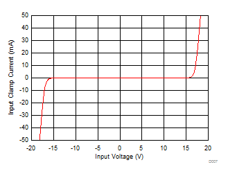
The ADS9212 features an internal clamp protection circuit on each of the two analog input channels; see Figure 6-1. The input clamp protection circuit allows each analog input to swing up to a maximum voltage of ±18V. Beyond an input voltage of ±18V, the input clamp circuit turns on and still operates from the single 5V supply. Figure 6-2 shows a typical current versus voltage characteristic curve for the input clamp.

For input voltages above the clamp threshold, make sure that the input current never exceeds ±10mA. A resistor placed in series with the analog inputs is an effective way to limit the input current. In addition to limiting the input current, the series resistor can also provide an antialiasing, low-pass filter (LPF) when coupled with a capacitor. Matching the external source impedance on the AINxP and AINxM pins cancels any additional offset error.
ADS9212 Input Protection Clamp
                    Profile, Input Clamp Current vs Source Voltage Figure 6-2 Input Protection Clamp Profile, Input Clamp Current vs Source Voltage