Typical values at TA = +25°C with
nominal supplies. Unless otherwise noted, TX input data rate = 491.52 MSPS,
fDAC = 11796.48 MSPS, interleave mode, AOUT = –1
dBFS, 1st Nyquist zone output, Internal PLL, fREF = 491.52
MSPS, 24x Interpolation, DSA = 0 dB, Sin(x)/x enabled, DSA calibrated.

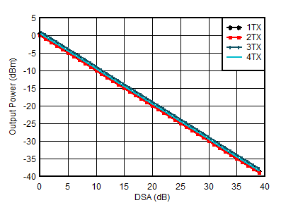
| Aout = -0.5 dFBS, 3.5 GHz Matching,
included PCB and cable losses |
|
Figure 7-453 TX
Output Power vs DSA Setting at 3.5 GHz
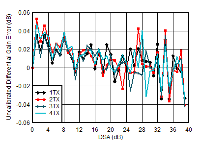
| 3.5
GHz Matching, included PCB and cable losses |
| Differential Gain Error = POUT(DSA Setting –
1) – POUT(DSA Setting) + 1 |
Figure 7-455 TX
Uncalibrated Differential Gain Error vs DSA Setting and Channel at 3.5
GHz
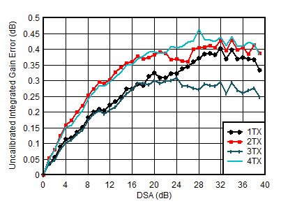
| 3.5
GHz Matching, included PCB and cable losses |
| Integrated Gain Error = POUT(DSA Setting) –
POUT(DSA Setting = 0) + (DSA
Setting) |
Figure 7-457 TX
Uncalibrated Integrated Gain Error vs DSA Setting and Channel at 3.5
GHz
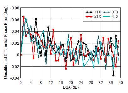
| 3.5
GHz Matching, included PCB and cable losses |
| Differential Phase Error = PhaseOUT(DSA
Setting – 1) – PhaseOUT(DSA Setting) |
Figure 7-459 TX
Uncalibrated Differential Phase Error vs DSA Setting and Channel at 3.5
GHz
| 3.5
GHz Matching, included PCB and cable losses |
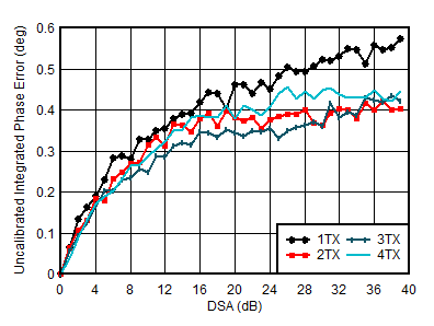
| Integrated Phase Error = Phase(DSA Setting) – Phase(DSA
Setting = 0) |
Figure 7-461 TX
Uncalibrated Integrated Phase Error vs DSA Setting and Channel at 3.5
GHz
| 3.5
GHz Matching, 1TX |
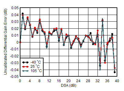
| Differential Phase Error = PhaseOUT(DSA
Setting – 1) – PhaseOUT(DSA Setting) |
Figure 7-463 TX
Uncalibrated Differential Gain Error vs DSA Setting and Temperature at 3.5
GHz
| 3.5
GHz Matching, 1TX |
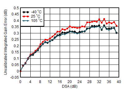
| Integrated Phase Error = Phase(DSA Setting) – Phase(DSA
Setting = 0) |
Figure 7-465 TX
Uncalibrated Integrated Gain Error vs DSA Setting and Temperature at 3.5
GHz
| 3.5
GHz Matching, 1TX |
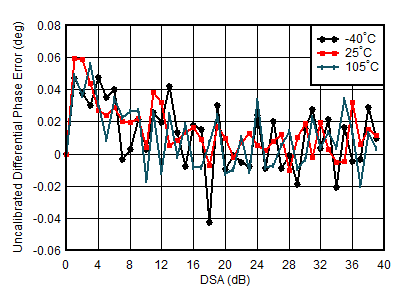
| Differential Phase Error = PhaseOUT(DSA
Setting – 1) – PhaseOUT(DSA Setting) |
Figure 7-467 TX
Uncalibrated Differential Phase Error vs DSA setting and Temperature at 3.5
GHz
| 3.5
GHz Matching, 1TX |
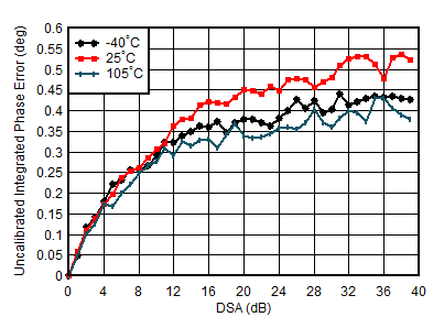
| Integrated Phase Error = Phase(DSA Setting) – Phase(DSA
Setting=0) |
Figure 7-469 TX
Uncalibrated Integrated Phase Error vs DSA Setting and Temperature at 3.5
GHz
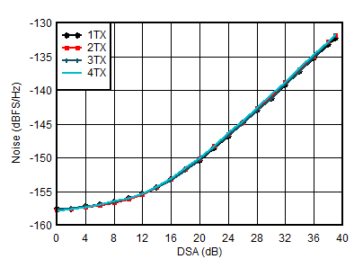
A.
| fDAC=11796.48 MSPS, interleave mode,
matching at 3.5 GHz, Aout = –13 dBFS. |
|
Figure 7-471 TX
NSD vs DSA Setting at 3.5 GHz
A.
| fDAC = 12 MSPS, external clock mode,
non-interleave mode |
|
Figure 7-473 TX
NSD vs Digital Amplitude and Channel at 3.75 GHz
| 20-MHz
tone spacing, 3.5 GHz Matching |
|
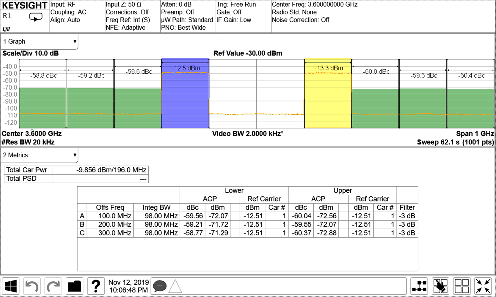
Figure 7-475 TX
IMD3 vs Digital Amplitude and Channel at 3.5 GHz
| External clock mode, non-interleave mode |
|
Figure 7-477 TX
IMD3 vs Tone Spacing and Channel at 3.75 GHz
| Inband
= 3.75 GHz ± 600 MHz, fDAC = 9 GSPS, external
clock mode, non-interleave mode. |
|
Figure 7-479 Two
Tone Inband SFDR vs Digital Amplitude at 3.75 GHz
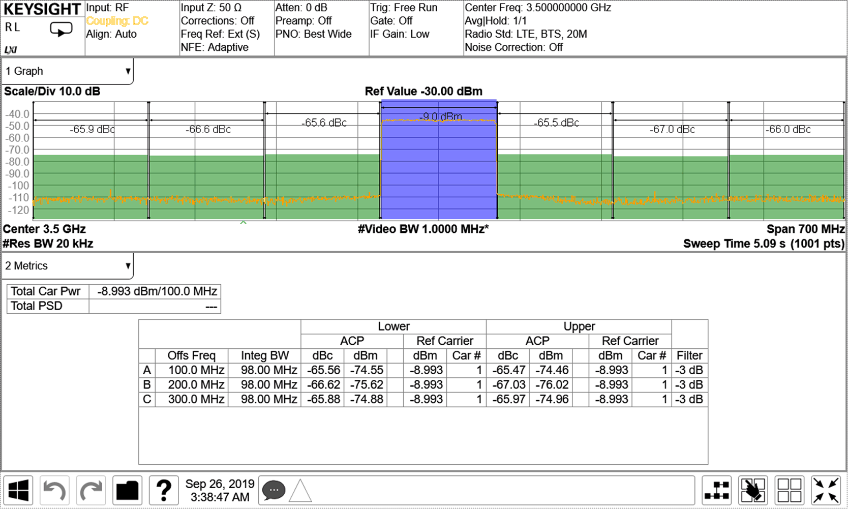
| 3.5
GHz Matching, single carrier 100-MHz BW NR TM1.1 |
Figure 7-481 TX
100-MHz NR Output Spectrum at 3.5 GHz (Band 42)
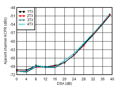
| 3.5
GHz Matching, single carrier 20-MHz BW NR TM1.1
LTE |
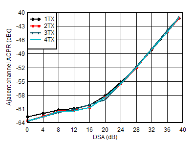
Figure 7-483 TX
20-MHz LTE ACPR vs DSA Setting at 3.5 GHz
| 3.5
GHz Matching, single carrier 100-MHz BW NR TM1.1 |
Figure 7-485 TX
100-MHz NR ACPR vs DSA Setting at 3.5 GHz
| 3.5
GHz Matching, single carrier 20-MHz BW TM1.1 LTE |
|
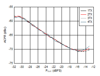
Figure 7-487 TX
20-MHz LTE ACPR vs Digital Level at 3.5 GHz
| 3.5
GHz Matching, single carrier 100-MHz BW NR TM1.1 |
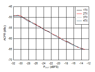
Figure 7-489 TX
100-MHz NR ACPR vs Digital Level at 3.5 GHz
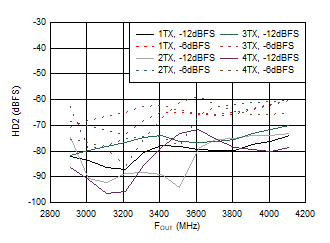
| Matching at 3.5 GHz, fDAC = 11.79648 GSPS,
interleave mode, normalized to output power at harmonic
frequency |
Figure 7-491 TX
Single Tone HD2 vs Frequency and Digital Level at 3.5 GHz
| Matching at 3.5 GHz, fDAC = 11.79648 GSPS,
interleave mode. |
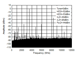
|
Figure 7-493 TX
Single Tone (–1 dBFS) Output Spectrum at 3.5 GHz (0 -
fDAC)
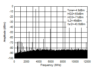
| Matching at 3.5 GHz, fDAC = 11.79648 GSPS,
interleave mode. |
Figure 7-495 TX
Single Tone (–6 dBFS) Output Spectrum at 3.5 GHz (0-fDAC)
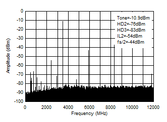
| Matching at 3.5 GHz, fDAC = 11.79648 GSPS,
interleave mode. |
Figure 7-497 TX
Single Tone (–12 dBFS) Output Spectrum at 3.5 GHz
(0-fDAC)
| Matching at 3.5 GHz, 50 MHz tone spacing,
fDAC = 12 GSPS, non-interleave
mode. |
|
Figure 7-499 TX
Dual Tone Output Spectrum at 3.75 GHz, -7 dBFS each (0 -
fDAC)
| Matching at 3.5 GHz, 50 MHz tone spacing,
fDAC = 12 GSPS, non-interleave
mode. |
|
Figure 7-501 TX
Dual Tone Output Spectrum at 3.75 GHz, -13 dBFS each (0 -
fDAC)
| Matching at 3.5 GHz, 50 MHz tone spacing,
fDAC = 12 GSPS, non-interleave
mode. |
|
Figure 7-503 TX
Dual Tone Output Spectrum at 3.75 GHz, -30 dBFS each (0 -
fDAC)
| fDAC = fCLK = 12 GSPS,
non-interleave mode. |
|
Figure 7-505 External Clock Additive Phase Noise at 3.7 GHz
| Aout = -0.5 dFBS, 3.5 GHz Matching,
included PCB and cable losses |
|
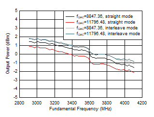
|
Figure 7-454 TX
Output Power vs Frequency
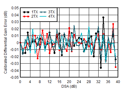
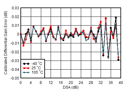
| 3.5
GHz Matching, included PCB and cable losses |
| Differential Gain Error = POUT(DSA Setting –
1) – POUT(DSA Setting) + 1 |
Figure 7-456 TX
Calibrated Differential Gain Error vs DSA Setting and Channel at 3.5
GHz
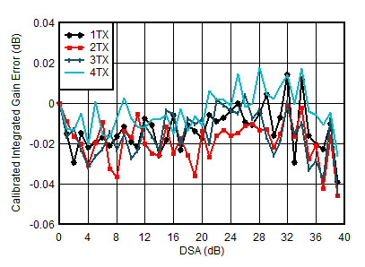
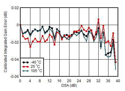
| 3.5
GHz Matching, included PCB and cable losses |
| Integrated Gain Error = POUT(DSA Setting) –
POUT(DSA Setting = 0) + (DSA
Setting) |
Figure 7-458 TX
Calibrated Integrated Gain Error vs DSA Setting and Channel at 3.5
GHz
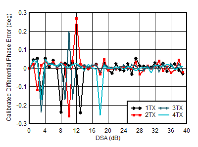
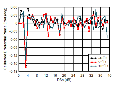
| 3.5
GHz Matching, included PCB and cable losses |
| Differential Phase Error = PhaseOUT(DSA
Setting – 1) – PhaseOUT(DSA Setting). Phase
DNL spike may occur at any DSA setting. |
Figure 7-460 TX
Calibrated Differential Phase Error vs DSA Setting and Channel at 3.5
GHz
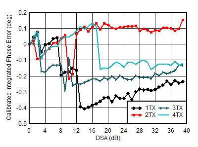
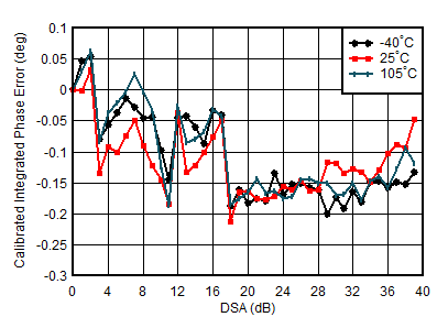
| 3.5
GHz Matching, included PCB and cable losses |
| Integrated Phase Error = Phase(DSA Setting) – Phase(DSA
Setting = 0) |
Figure 7-462 TX
Calibrated Integrated Phase Error vs DSA Setting and Channel at 3.5
GHz
| 3.5
GHz Matching, 1TX, Calibrated at 25°C |
| Differential Phase Error = PhaseOUT(DSA
Setting – 1) – PhaseOUT(DSA Setting) |
Figure 7-464 TX
Calibrated Differential Gain Error vs DSA Setting and Temperature at 3.5
GHz
| 3.5
GHz Matching, 1TX, Calibrated at 25°C |
| Integrated Phase Error = Phase(DSA Setting) – Phase(DSA
Setting = 0) |
Figure 7-466 TX
Calibrated Integrated Gain Error vs DSA Setting and Temperature at 3.5
GHz
| 3.5
GHz Matching, 1TX, Calibrated at 25°C |
| Differential Phase Error = PhaseOUT(DSA
Setting – 1) – PhaseOUT(DSA Setting) |
Figure 7-468 TX
Calibrated Differential Phase Error vs DSA Setting and Temperature at 3.5
GHz
| 3.5
GHz Matching, 1TX, Calibrated at 25°C |
| Integrated Phase Error = Phase(DSA Setting) – Phase(DSA
Setting = 0) |
Figure 7-470 TX
Calibrated Integrated Phase Error vs DSA Setting and Temperature at 3.5
GHz
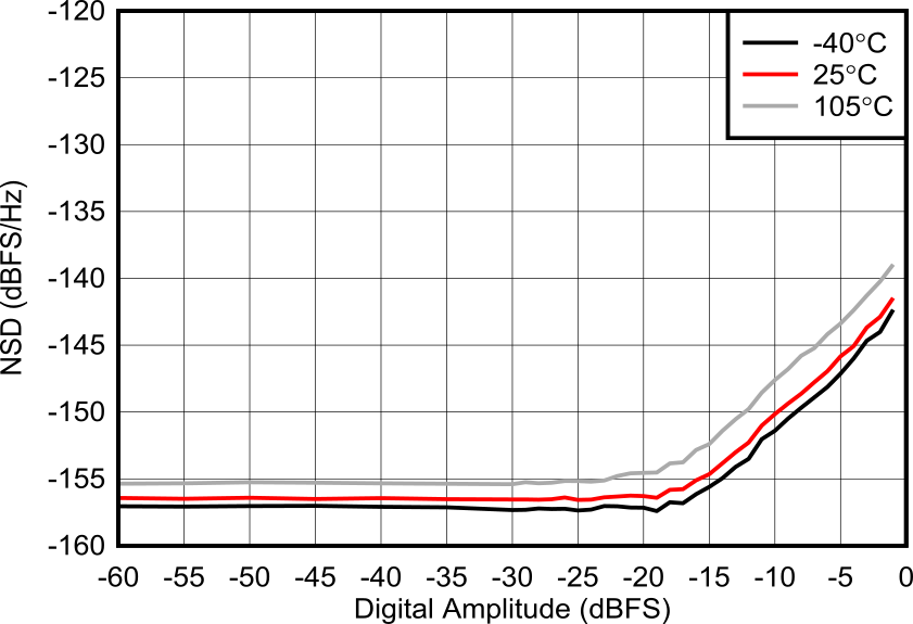
A.
| fDAC = 12 MSPS, external clock mode,
non-interleave mode |
|
Figure 7-472 TX
NSD vs Digital Amplitude and Temperature at 3.75 GHz
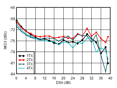
| 20-MHz
tone spacing, 3.5 GHz Matching, –13 dBFS each tone,
included PCB and cable losses |
|
Figure 7-474 TX
IMD3 vs DSA Setting at 3.5 GHz
| 50-MHz
tone spacing, external clock mode, non-interleave
mode |
|
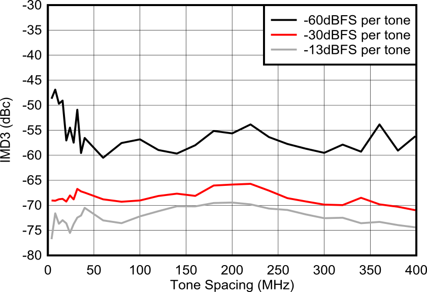
Figure 7-476 TX
IMD3 vs Tone Spacing and Amplitude at 3.75 GHz
| 50-MHz
tone spacing, external clock mode, non-interleave
mode |
|
Figure 7-478 TX
IMD3 vs Digital Amplitude and Temperature at 3.75 GHz
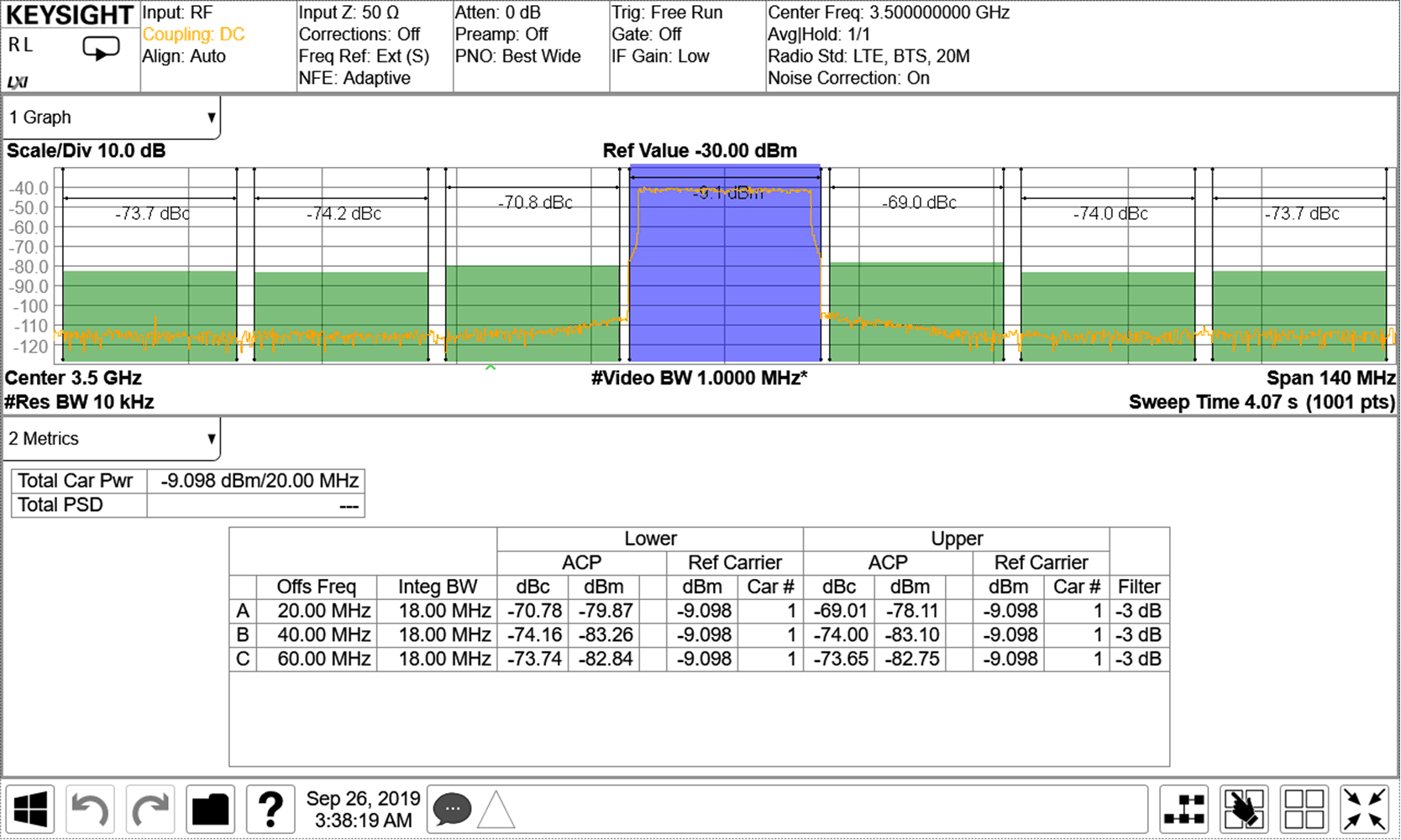
| 3.5
GHz Matching, single carrier 20-MHz BW TM1.1 LTE |
Figure 7-480 TX
20-MHz LTE Output Spectrum at 3.5 GHz (Band 42)
| 3.5
GHz Matching, single carrier 100-MHz BW NR TM1.1 |
Figure 7-482 TX 2
carrier 100-MHz NR Output Spectrum at 3.45 GHz and 3.75 GHz
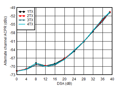
| 3.5
GHz Matching, single carrier 20-MHz BW TM1.1 LTE |
Figure 7-484 TX
20-MHz LTE alt-ACPR vs DSA Setting at 3.5 GHz
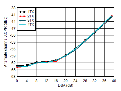
| 3.5
GHz Matching, single carrier 100-MHz BW NR TM1.1 |
Figure 7-486 TX
100-MHz NR alt-ACPR vs DSA Setting at 3.5 GHz
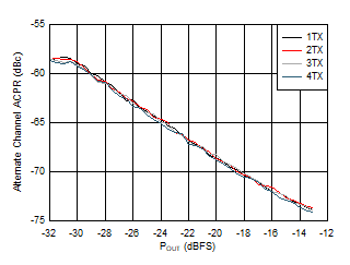
| 3.5
GHz Matching, single carrier 20-MHz BW TM1.1 LTE |
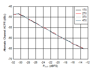
Figure 7-488 TX
20-MHz LTE alt-ACPR vs Digital Level at 3.5 GHz
| 3.5
GHz Matching, single carrier 100-MHz BW NR TM1.1 |
|
Figure 7-490 TX
100-MHz NR alt-ACPR vs Digital Level at 3.5 GHz
| Matching at 3.5 GHz, fDAC = 11.79648 GSPS,
interleave mode, normalized to output power at harmonic
frequency. Dip is due to HD3 falling near DC. |
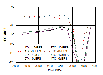
Figure 7-492 TX
Single Tone HD3 vs Frequency and Digital Level at 3.5 GHz
| Matching at 3.5 GHz, fDAC = 11.79648 GSPS,
interleave mode. |
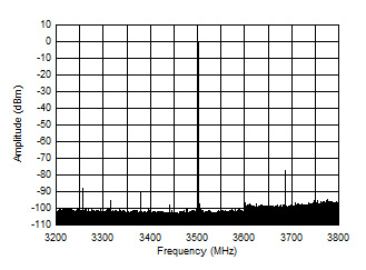
Figure 7-494 TX
Single Tone (–1 dBFS) Output Spectrum at 3.5 GHz (±300 MHz)
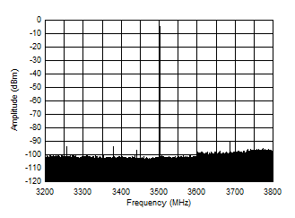
| Matching at 3.5 GHz, fDAC = 11.79648 GSPS,
interleave mode. |
Figure 7-496 TX
Single Tone (–6 dBFS) Output Spectrum at 3.5 GHz (±300 MHz)
| Matching at 3.5 GHz, fDAC = 11.79648 GSPS,
interleave mode. |
|
Figure 7-498 TX
Single Tone (–12 dBFS) Output Spectrum at 3.5 GHz (±300 MHz)
| Matching at 3.5 GHz, 50 MHz tone spacing,
fDAC = 12 GSPS, non-interleave
mode. |
|
Figure 7-500 TX
Dual Tone Output Spectrum at 3.75 GHz, -7 dBFS each (±600 MHz)
| Matching at 3.5 GHz, 50 MHz tone spacing,
fDAC = 12 GSPS, non-interleave
mode. |
|
Figure 7-502 TX
Dual Tone Output Spectrum at 3.75 GHz, -13 dBFS each (±600 MHz)
| Matching at 3.5 GHz, 50 MHz tone spacing,
fDAC = 12 GSPS, non-interleave
mode. |
|
Figure 7-504 TX
Dual Tone Output Spectrum at 3.75 GHz, -30 dBFS each (±600 MHz)