Typical values at TA =
+25°C with nominal supplies. Default conditions: TX input data rate = 491.52MSPS,
fDAC = 11796.48MSPS (24x interpolation), interleave mode,
1st Nyquist zone output, PLL clock mode with fREF = 491.52
MHz, AOUT = –1 dBFS, DSA = 0 dB, Sin(x)/x enabled, DSA calibrated, TX
Clock Dither Enabled

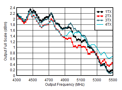
| Excluding PCB and cable losses, Aout =
-0.5dFBS, DSA = 0, 4.9 GHz matching |
Figure 6-149 TX
Full Scale vs RF Frequency and Channel at 11796.48MSPS
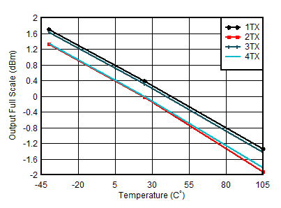
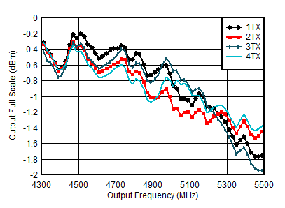
| fDAC = 11796.48 MSPS, Aout =
-0.5dFBS, matching 4.9 GHz |
|
Figure 6-151 TX
Output Power vs DSA Setting and Channel at 4.9 GHz
| fDAC=11796.48MSPS, interleave mode,
matching at 4.9 GHz |
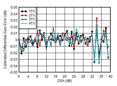
| Differential Gain Error = POUT(DSA Setting –
1) – POUT(DSA Setting) + 1 |
Figure 6-153 TX
Calibrated Differential Gain Error vs DSA Setting and Channel at 4.9
GHz
| fDAC = 11796.48MSPS, interleave mode,
matching at 4.9 GHz |
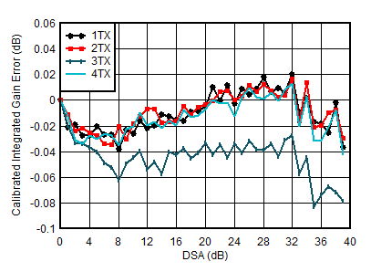
| Integrated Gain Error = POUT(DSA Setting) –
POUT(DSA Setting = 0) + (DSA
Setting) |
|
Figure 6-155 TX
Calibrated Integrated Gain Error vs DSA Setting and Channel at 4.9
GHz
| fDAC = 11796.48MSPS, interleaved mode,
matching at 4.9 GHz |
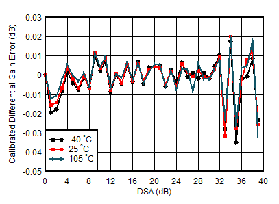
| Differential Gain Error = POUT(DSA Setting –
1) – POUT(DSA Setting) + 1 |
Figure 6-157 TX
Calibrated Differential Gain Error vs DSA Setting and Temperature at 4.9
GHz
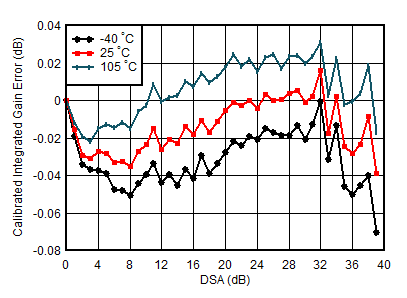
| fDAC = 11796.48MSPS, interleaved mode,
matching at 4.9 GHz |
| Integrated Gain Error = POUT(DSA Setting) –
POUT(DSA Setting = 0) + (DSA
Setting) |
Figure 6-159 TX
Calibrated Integrated Gain Error vs DSA Setting and Temperature at 4.9
GHz
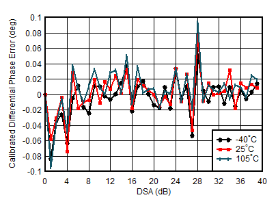
| fDAC = 11796.48MSPS, interleaved mode,
matching at 4.9 GHz |
| Differential Phase Error = PhaseOUT(DSA
Setting – 1) – PhaseOUT(DSA Setting) |
| Phase
DNL spike may occur at any DSA setting. |
Figure 6-161 TX
Calibrated Differential Phase Error vs DSA Setting and Channel at 4.9
GHz
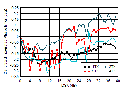
| fDAC = 11796.48MSPS, interleaved mode,
matching at 4.9 GHz |
| Integrated Phase Error = Phase(DSA Setting) – Phase(DSA
Setting = 0) |
Figure 6-163 TX
Calibrated Integrated Phase Error vs DSA Setting and Channel at 4.9
GHz
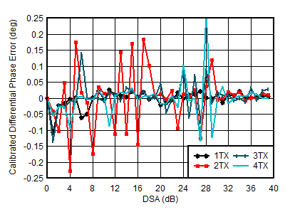
| fDAC = 11796.48MSPS, interleaved mode,
matching at 4.9 GHz |
| Differential Phase Error = PhaseOUT(DSA
Setting – 1) – PhaseOUT(DSA Setting) |
Figure 6-165 TX
Calibrated Differential Phase Error vs DSA Setting and Temperature at 4.9
GHz
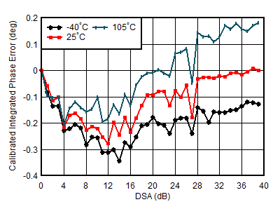
| fDAC = 11796.48MSPS, interleaved mode,
matching at 4.9 GHz, channel with the median variation
over DSA setting at 25°C |
| Integrated Phase Error = Phase(DSA Setting) – Phase(DSA
Setting = 0) |
Figure 6-167 TX
Calibrated Integrated Phase Error vs DSA Setting and Temperature at 4.9
GHz
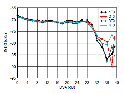
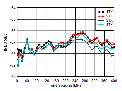
| fDAC = 11796.48MSPS, interleaved mode,
matching at 4.9 GHz, fCENTER = 4.9GHz, -13
dBFS each tone |
Figure 6-169 TX
IMD3 vs DSA Setting at 4.9 GHz
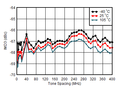
| fDAC = 11796.48MSPS, interleaved mode,
matching at 4.9 GHz, fCENTER = 4.9GHz, –13
dBFS each tone, worst channel |
Figure 6-171 TX
IMD3 vs Tone Spacing and Temperature at 4.9 GHz
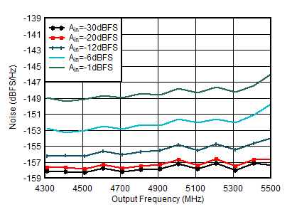
| Matching at 4.9 GHz, Single tone, fDAC =
11.79648GSPS, interleave mode, 40-MHz offset,
DSA=0dB |
Figure 6-173 TX
Single Tone Output Noise vs Frequency and Amplitude at 4.9 GHz
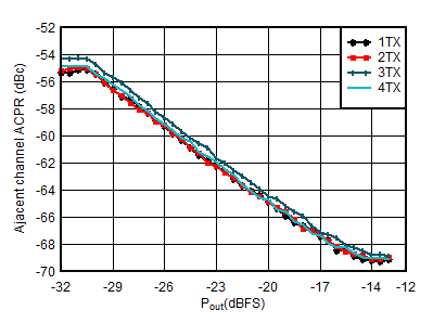
| Matching at 4.9 GHz, single carrier 20-MHz BW TM1.1
LTE |
Figure 6-175 TX
20-MHz LTE ACPR vs Digital Level at 4.9 GHz
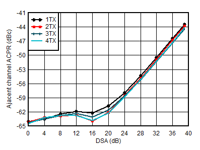
| Matching at 4.9 GHz, single carrier 20-MHz BW TM1.1
LTE |
Figure 6-177 TX
20-MHz LTE ACPR vs DSA at 4.9 GHz
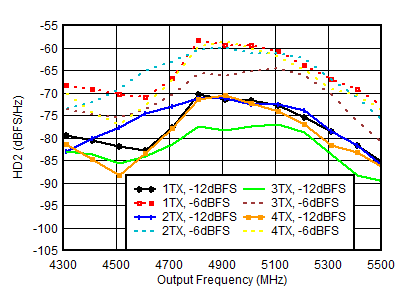
| Matching at 4.9 GHz, fDAC = 11.79648GSPS,
interleave mode, normalized to output power at harmonic
frequency |
Figure 6-179 TX
HD2 vs Digital Amplitude and Output Frequency at 4.9 GHz
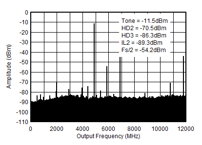
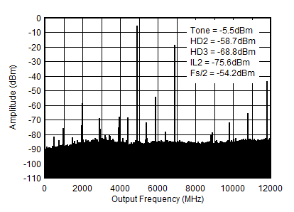
| fDAC = 11796.48MSPS, interleave mode,
4.9 GHz matching, includes PCB and cable losses. ILn =
fS/n ± fOUT. |
Figure 6-181 TX
Single Tone (–12 dBFS) Output Spectrum at 4.9 GHz
(0-fDAC)
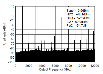
| fDAC = 11796.48MSPS, interleave mode,
4.9 GHz matching, includes PCB and cable losses. ILn =
fS/n ± fOUT. |
Figure 6-183 TX
Single Tone (–1 dBFS) Output Spectrum at 4.9 GHz (0-fDAC)
| Excluding PCB and cable losses, Aout =
-0.5dFBS, DSA = 0, 4.9 GHz matching |
Figure 6-150 TX
Full Scale vs RF Frequency and Channel at 5898.24MSPS, Straight Mode, 2nd
Nyquist Zone
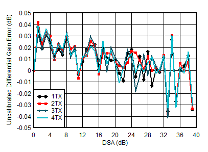
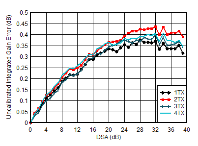
| fDAC=11796.48MSPS, interleave mode,
matching at 4.9 GHz |
| Differential Gain Error = POUT(DSA Setting –
1) – POUT(DSA Setting) + 1 |
Figure 6-152 TX
Uncalibrated Differential Gain Error vs DSA Setting and Channel at 4.9
GHz
| fDAC=11796.48MSPS, interleave mode,
matching at 4.9 GHz |
| Integrated Gain Error = POUT(DSA Setting) –
POUT(DSA Setting = 0) + (DSA
Setting) |
Figure 6-154 TX
Uncalibrated Integrated Gain Error vs DSA Setting and Channel at 4.9
GHz
| fDAC = 11796.48MSPS, interleaved mode,
matching at 4.9 GHz |
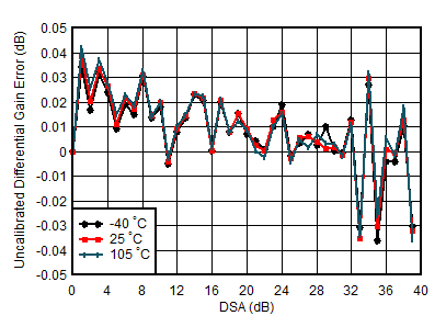
| Differential Gain Error = POUT(DSA Setting –
1) – POUT(DSA Setting) + 1 |
Figure 6-156 TX
Uncalibrated Differential Gain Error vs DSA Setting and Temperature at 4.9
GHz
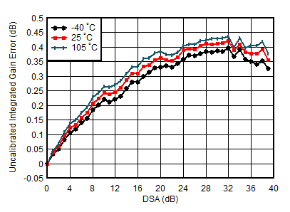
| fDAC = 11796.48MSPS, interleaved mode,
matching at 4.9 GHz |
| Integrated Gain Error = POUT(DSA Setting) –
POUT(DSA Setting = 0) + (DSA
Setting) |
Figure 6-158 TX
Uncalibrated Integrated Gain Error vs DSA Setting and Temperature at 4.9
GHz
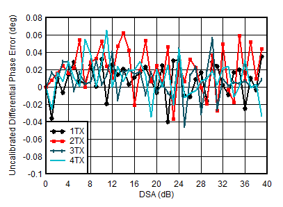
| fDAC = 11796.48MSPS, interleaved mode,
matching at 4.9 GHz |
| Differential Phase Error = PhaseOUT(DSA
Setting – 1) – PhaseOUT(DSA Setting) |
Figure 6-160 TX
Uncalibrated Differential Phase Error vs DSA Setting and Channel at 4.9
GHz
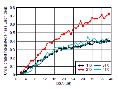
| fDAC = 11796.48MSPS, interleaved mode,
matching at 4.9 GHz |
| Integrated Phase Error = Phase(DSA Setting) – Phase(DSA
Setting = 0) |
|
Figure 6-162 TX
Uncalibrated Integrated Phase Error vs DSA Setting and Channel at 4.9
GHz
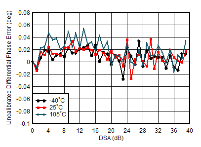
| fDAC = 11796.48MSPS, interleaved mode,
matching at 4.9 GHz |
| Differential Phase Error = PhaseOUT(DSA
Setting – 1) – PhaseOUT(DSA Setting) |
Figure 6-164 TX
Uncalibrated Differential Phase Error vs DSA Setting and Temperature at 4.9
GHz
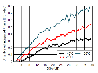
| fDAC = 11796.48MSPS, interleaved mode,
matching at 4.9 GHz |
| Integrated Phase Error = Phase(DSA Setting) – Phase(DSA
Setting = 0) |
Figure 6-166 TX
Uncalibrated Integrated Phase Error vs DSA Setting and Temperature at 4.9
GHz
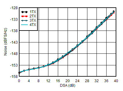
| fDAC = 11796.48MSPS, interleaved mode,
matching at 4.9 GHz, POUT = –13 dBFS |
|
|
|
Figure 6-168 TX
Output Noise vs Channel and Attenuation at 2.6 GHz
| fDAC = 11796.48MSPS, interleaved mode,
matching at 4.9 GHz, fCENTER = 4.9GHz, –13
dBFS each tone |
Figure 6-170 TX
IMD3 vs Tone Spacing and Channel at 4.9 GHz
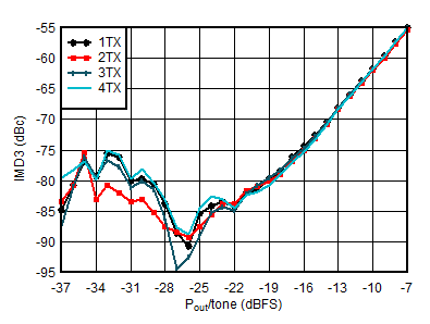
| fDAC = 11796.48MSPS, interleaved mode,
matching at 4.9 GHz, fCENTER = 4.9GHz,
fSPACING = 20 MHz |
Figure 6-172 TX
IMD3 vs Digital Level at 4.9 GHz
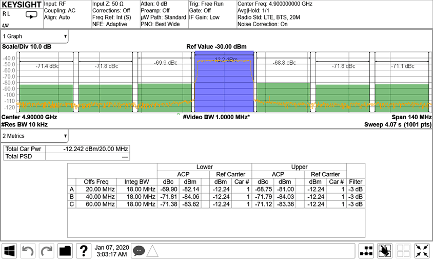
| TM1.1,
POUT_RMS = –13 dBFS |
|
Figure 6-174 TX
20-MHz LTE Output Spectrum at 4.9 GHz
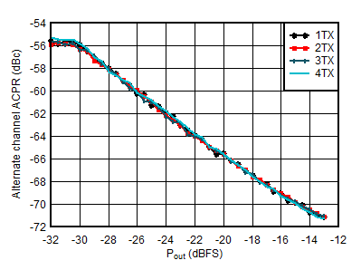
| Matching at 4.9 GHz, single carrier 20-MHz BW TM1.1
LTE |
Figure 6-176 TX
20-MHz LTE alt-ACPR vs Digital Level at 4.9 GHz
| Matching at 4.9 GHz, single carrier 20-MHz BW TM1.1
LTE |
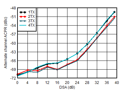
Figure 6-178 TX
20-MHz LTE alt-ACPR vs DSA at 4.9 GHz
| Matching at 4.9 GHz, fDAC = 11.79648GSPS,
interleave mode, normalized to output power at harmonic
frequency |
|
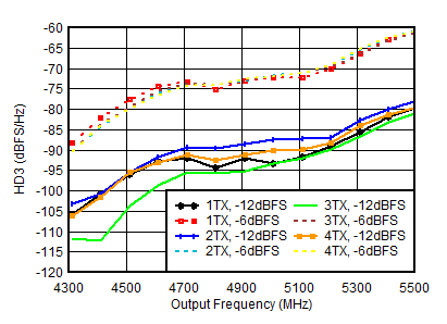
Figure 6-180 TX
HD3 vs Digital Amplitude and Output Frequency at 4.9 GHz
| fDAC = 11796.48MSPS, interleave mode,
4.9 GHz matching, includes PCB and cable losses. ILn =
fS/n ± fOUT. |
Figure 6-182 TX
Single Tone (–6 dBFS) Output Spectrum at 4.9 GHz (0-fDAC)
