Typical values at TA = +25°C with
nominal supplies. Default conditions: TX input data rate = 491.52 MSPS,
fDAC = 11796.48 MSPS (24x interpolation), interleave mode,
1st Nyquist zone output, PLL clock mode with fREF = 491.52
MHz, AOUT = –1 dBFS, DSA = 0 dB, Sin(x)/x enabled, DSA calibrated

| including PCB and cable losses, Aout = -0.5
dFBS, DSA = 0, 1.8 GHz matching |
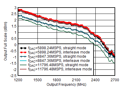
Figure 5-44 TX
Output Fullscale vs Output Frequency
| fDAC = 5898.24 MSPS, interleave mode,
matching at 1.8 GHz |
| Differential Gain Error = POUT(DSA Setting –
1) – POUT(DSA Setting) + 1 |
Figure 5-46 TX
Uncalibrated Differential Gain Error vs DSA Setting and Channel at 1.8
GHz
| fDAC = 5898.24 MSPS, interleave mode,
matching at 1.8 GHz |
| Integrated Gain Error = POUT(DSA Setting) –
POUT(DSA Setting = 0) + (DSA
Setting) |
Figure 5-48 TX
Uncalibrated Integrated Gain Error vs DSA Setting and Channel at 1.8
GHz
| fDAC = 5898.24 MSPS, interleave mode,
matching at 1.8 GHz |
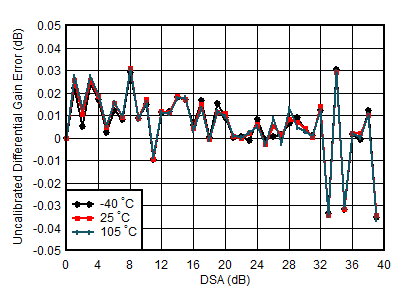
| Differential Gain Error = POUT(DSA Setting –
1) – POUT(DSA Setting) + 1 |
Figure 5-50 TX
Uncalibrated Differential Gain Error vs DSA Setting and Temperature at 1.8
GHz
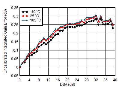
| fDAC = 5898.24 MSPS, interleave mode,
matching at 1.8 GHz |
| Integrated Gain Error = POUT(DSA Setting) –
POUT(DSA Setting = 0) + (DSA
Setting) |
Figure 5-52 TX
Uncalibrated Integrated Gain Error vs DSA Setting and Temperature at 1.8
GHz
| fDAC = 5898.24 MSPS, interleave mode,
matching at 1.8 GHz |
| Differential Phase Error = PhaseOUT(DSA
Setting – 1) – PhaseOUT(DSA Setting) |
Figure 5-54 TX
Uncalibrated Differential Phase Error vs DSA Setting and Channel at 1.8
GHz
| fDAC = 5898.24 MSPS, interleave mode,
matching at 1.8 GHz |
| Integrated Phase Error = Phase(DSA Setting) – Phase(DSA
Setting = 0) |
Figure 5-56 TX
Uncalibrated Integrated Phase Error vs DSA Setting and Channel at 1.8
GHz
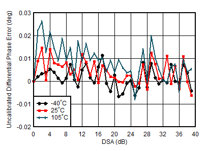
| fDAC = 5898.24 MSPS, interleave mode,
matching at 1.8 GHz |
| Differential Phase Error = PhaseOUT(DSA
Setting – 1) – PhaseOUT(DSA Setting) |
Figure 5-58 TX
Uncalibrated Differential Phase Error vs DSA Setting and Temperature at 1.8
GHz
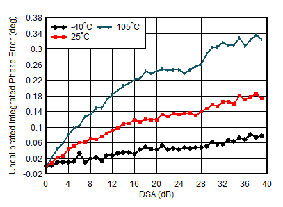
| fDAC = 5898.24MSPS, interleave mode,
matching at 1.8 GHz, channel with the median variation
over DSA setting at 25°C |
| Integrated Phase Error = Phase(DSA Setting) – Phase(DSA
Setting = 0) |
Figure 5-60 TX
Uncalibrated Integrated Phase Error vs DSA Setting and Temperature at 1.8
GHz
| fDAC = 5898.24 MSPS, interleave mode,
matching at 1.8 GHz, POUT = –13 dBFS |
Figure 5-62 TX
Output Noise vs Channel and Attenuation at 1.8 GHz
| fDAC = 11796.48 MSPS, interleave mode,
fCENTER = 1.8 GHz, matching at 1.8 GHz,
–13 dBFS each tone |
Figure 5-64 TX
IMD3 vs Tone Spacing and Channel at 1.8 GHz
| fDAC = 11796.48 MSPS, interleave mode,
fCENTER = 1.8 GHz, fSPACING =
20 MHz, matching at 1.8 GHz |
Figure 5-66 TX
IMD3 vs Digital Level at 1.8 GHz
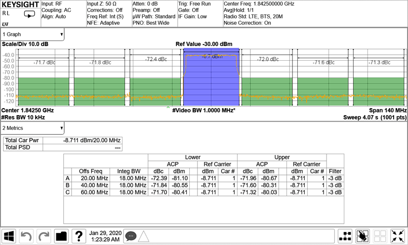
| TM1.1, POUT_RMS = –13 dBFS |

| Matching at 1.8 GHz, single carrier 20-MHz BW TM1.1
LTE |
Figure 5-70 TX
20-MHz LTE alt-ACPR vs Digital Level at 1.8425 GHz
| Matching at 1.8 GHz, single carrier 20-MHz BW TM1.1
LTE |
Figure 5-72 TX
20-MHz LTE alt-ACPR vs DSA at 1.8 GHz
| Matching at 1.8 GHz, fDAC = 11.79648 GSPS,
interleave mode, normalized to output power at harmonic
frequency |
Figure 5-74 TX
HD3 vs Digital Amplitude and Output Frequency at 1.8 GHz
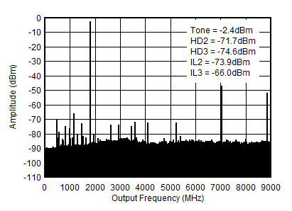
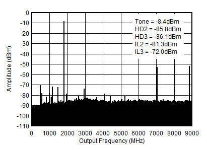
| fDAC = 8847.36 MSPS, straight mode,
1.8 GHz matching, includes PCB and cable losses. ILn =
fS/n ± fOUT and is due to
mixing with digital clocks. |

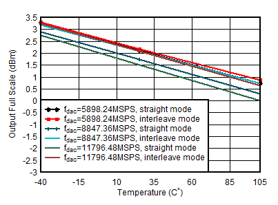
| Aout = -0.5 dFBS, matching 1.8
GHz |
Figure 5-45 TX
Output Power vs Temperature at 1.8 GHz
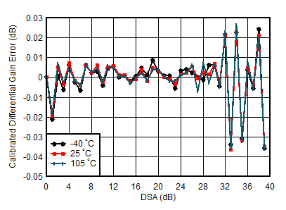
| fDAC = 5898.24 MSPS, interleave mode,
matching at 1.8 GHz |
| Differential Gain Error = POUT(DSA Setting –
1) – POUT(DSA Setting) + 1 |
Figure 5-47 TX
Calibrated Differential Gain Error vs DSA Setting and Channel at 1.8
GHz
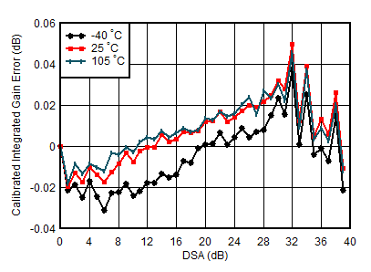
| fDAC = 5898.24 MSPS, interleave mode,
matching at 1.8 GHz |
| Integrated Gain Error = POUT(DSA Setting) –
POUT(DSA Setting = 0) + (DSA
Setting) |
Figure 5-49 TX
Calibrated Integrated Gain Error vs DSA Setting and Channel at 1.8
GHz
| fDAC = 5898.24 MSPS, interleave mode,
matching at 1.8 GHz |
| Differential Gain Error = POUT(DSA Setting –
1) – POUT(DSA Setting) + 1 |
Figure 5-51 TX
Calibrated Differential Gain Error vs DSA Setting and Temperature at 1.8
GHz
| fDAC = 5898.24 MSPS, interleave mode,
matching at 1.8 GHz |
| Integrated Gain Error = POUT(DSA Setting) –
POUT(DSA Setting = 0) + (DSA
Setting) |
Figure 5-53 TX
Calibrated Integrated Gain Error vs DSA Setting and Temperature at 1.8
GHz
| fDAC = 8847.36 MSPS, straight mode,
matching at 2.6 GHz |
| Differential Phase Error = PhaseOUT(DSA
Setting – 1) – PhaseOUT(DSA Setting) |
| Phase
DNL spike may occur at any DSA setting. |
Figure 5-55 TX
Calibrated Differential Phase Error vs DSA Setting and Channel at 1.8
GHz
| fDAC = 5898.24 MSPS, interleave mode,
matching at 1.8 GHz |
| Integrated Phase Error = Phase(DSA Setting) – Phase(DSA
Setting = 0) |
Figure 5-57 TX
Calibrated Integrated Phase Error vs DSA Setting and Channel at 1.8
GHz
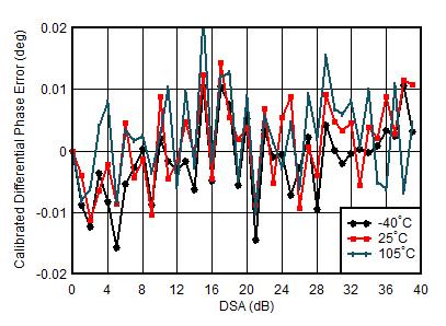
| fDAC = 5898.24 MSPS, interleave mode,
matching at 1.8 GHz, channel with the median variation
over DSA setting at 25°C |
| Differential Phase Error = PhaseOUT(DSA
Setting – 1) – PhaseOUT(DSA Setting) |
Figure 5-59 TX
Calibrated Differential Phase Error vs DSA Setting and Temperature at 1.8
GHz
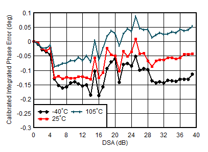
| fDAC = 5898.24 MSPS, interleave mode,
matching at 1.8 GHz, channel with the median variation
over DSA setting at 25°C |
| Integrated Phase Error = Phase(DSA Setting) – Phase(DSA
Setting = 0) |
Figure 5-61 TX
Calibrated Integrated Phase Error vs DSA Setting and Temperature at 1.8
GHz
| fDAC = 11796.48 MSPS, interleave mode,
fCENTER = 1.8 GHz, matching at 1.8 GHz,
–13 dBFS each tone |
Figure 5-63 TX
IMD3 vs DSA Setting at 1.8 GHz
| fDAC = 11796.48 MSPS, interleave mode,
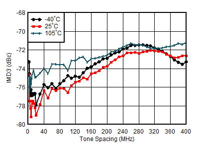
fCENTER = 1.8 GHz, matching at 1.8 GHz,
–13 dBFS each tone, worst channel |
Figure 5-65 TX
IMD3 vs Tone Spacing and Temperature at 1.8 GHz
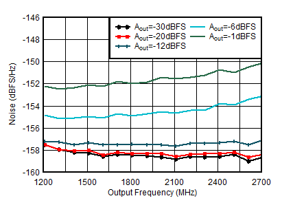
| Matching at 2.6 GHz, Single tone, fDAC =
11.79648GSPS, interleave mode, 40-MHz offset |
Figure 5-67 TX
Single Tone Output Noise vs Frequency and Amplitude at 1.8 GHz
| Matching at 1.8 GHz, single carrier 20-MHz BW TM1.1
LTE |
Figure 5-69 TX
20-MHz LTE ACPR vs Digital Level at 1.8425 GHz
| Matching at 1.8 GHz, single carrier 20-MHz BW TM1.1
LTE |
Figure 5-71 TX
20-MHz LTE ACPR vs DSA at 1.8 GHz
| Matching at 1.8 GHz, fDAC = 11.79648 GSPS,
interleave mode, normalized to output power at harmonic
frequency |
Figure 5-73 TX
HD2 vs Digital Amplitude and Output Frequency at 1.8 GHz
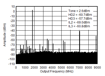
| fDAC = 8847.36 MSPS, straight mode,
1.8 GHz matching, includes PCB and cable losses. ILn =
fS/n ± fOUT and is due to
mixing with digital clocks. |

| fDAC = 8847.36 MSPS, straight mode,
1.8 GHz matching, includes PCB and cable losses. ILn =
fS/n ± fOUT and is due to
mixing with digital clocks. |
