JAJSHC9B May   2019  – October 2021 ALM2402F-Q1

PRODUCTION DATA  

  1. 特長
  2. アプリケーション
  3. 概要
  4. Revision History
  5. Pin Configuration and Functions
  6. Specifications
    1. 6.1 Absolute Maximum Ratings
    2. 6.2 ESD Ratings
    3. 6.3 Recommended Operating Conditions
    4. 6.4 Thermal Information
    5. 6.5 Electrical Characteristics: VS = 12 V
    6. 6.6 Electrical Characteristics: VS = 5 V
    7. 6.7 Typical Characteristics
  7. Detailed Description
    1. 7.1 Overview
    2. 7.2 Functional Block Diagram
    3. 7.3 Feature Description
      1. 7.3.1 OTF/SH_DN
      2. 7.3.2 Output Stage Supply Voltage
      3. 7.3.3 Current-Limit and Short-Circuit Protection
      4. 7.3.4 Input Common-Mode Overvoltage Clamps
      5. 7.3.5 Thermal Shutdown
      6. 7.3.6 Output Stage
      7. 7.3.7 EMI Susceptibility and Input Filtering
    4. 7.4 Device Functional Modes
      1. 7.4.1 Open-Loop and Closed-Loop Operation
      2. 7.4.2 Shutdown
  8. Application and Implementation
    1. 8.1 Application Information
      1. 8.1.1 Capacitive Load and Stability
    2. 8.2 Typical Application
      1. 8.2.1 Design Requirements
      2. 8.2.2 Detailed Design Procedure
        1. 8.2.2.1 Resolver Excitation Input (Op Amp Output)
          1. 8.2.2.1.1 Excitation Voltage
          2. 8.2.2.1.2 Excitation Frequency
          3. 8.2.2.1.3 Excitation Impedance
        2. 8.2.2.2 Resolver Output
        3. 8.2.2.3 Power Dissipation and Thermal Reliability
          1. 8.2.2.3.1 Improving Package Thermal Performance
      3. 8.2.3 Application Curves
  9. Power Supply Recommendations
  10. 10Layout
    1. 10.1 Layout Guidelines
    2. 10.2 Layout Example
  11. 11Device and Documentation Support
    1. 11.1 Documentation Support
      1. 11.1.1 Related Documentation
    2. 11.2 Receiving Notification of Documentation Updates
    3. 11.3 サポート・リソース
    4. 11.4 Trademarks
    5. 11.5 Electrostatic Discharge Caution
    6. 11.6 Glossary
  12. 12Mechanical, Packaging, and Orderable Information

パッケージ・オプション

メカニカル・データ(パッケージ|ピン)
サーマルパッド・メカニカル・データ
発注情報

Application Curves

The THD+N performance for the circuit described in the Excitation Voltage section is measured for a 10-kHz, 10-VPP output signal from each op-amp channel. These measurement results are displayed in Table 8-2.

Table 8-2 Maximum Output Power and THD+N
LOAD IMPEDANCE
(Ω)
MAXIMUM OUTPUT POWER
(mW)
THD+N AT MAXIMUM OUTPUT POWER
(dB)
100292–50

Figure 8-4 shows the THD+N performance for different input signal frequencies with a measurement bandwidth of 80 kHz. Figure 8-5 shows the circuit response with load capacitances of up to 100 nF. Using a larger resistor in series with the output, as shown in Section 8.1.1 further improves phase margin.
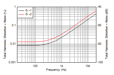
GUID-23ADA654-6802-4229-8B55-7F16961603BE-low.gifFigure 8-4 THD+N vs Frequency
GUID-C4124B25-AE91-4139-9CCD-419C47B959A6-low.gifFigure 8-5 Small-Signal Overshoot vs Capacitive Load