JAJSHC9B May 2019 – October 2021 ALM2402F-Q1
PRODUCTION DATA
- 1 特長
- 2 アプリケーション
- 3 概要
- 4 Revision History
- 5 Pin Configuration and Functions
- 6 Specifications
- 7 Detailed Description
- 8 Application and Implementation
- 9 Power Supply Recommendations
- 10Layout
- 11Device and Documentation Support
- 12Mechanical, Packaging, and Orderable Information
パッケージ・オプション
メカニカル・データ(パッケージ|ピン)
- PWP|14
サーマルパッド・メカニカル・データ
- PWP|14
発注情報
8.2.2.1.3 Excitation Impedance
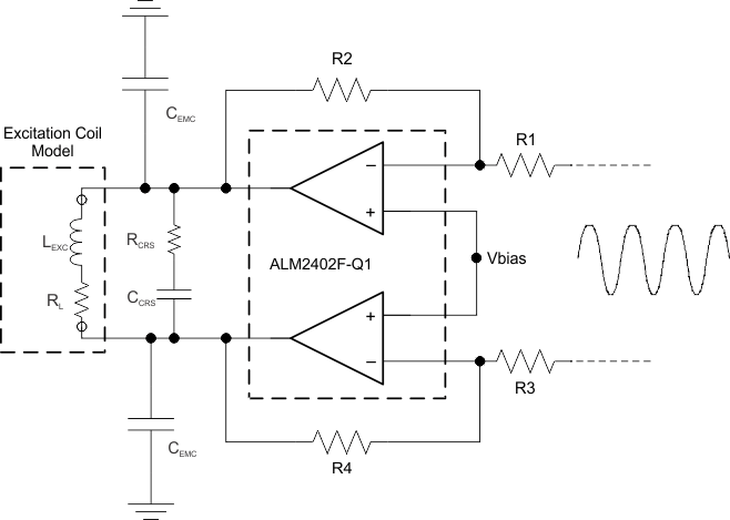
Knowledge of the primary-side impedance is very important when choosing an op amp for this application. As shown in Figure 8-3, the excitation coil looks like an inductance in series with a resistance. Often, these values are not given, or are given as a function of frequency or phase angle, and must by calculated from the Cartesian or polar form. This calculation is a trivial task.
After the coil resistance is determined, the maximum or peak-peak current needed from ALM2402F-Q1 is determined using Equation 2:

In this example, the peak-to-peak output current equates to approximately 100 mA. Each op amp handles the peak current, with one op amp sinking current while the other op amp is sourcing current. Knowledge of the op amp current is very important when determining the device power dissipation, a topic that is discussed in Power Dissipation and Thermal Reliability.
 Figure 8-3 Excitation Coil Implementation
As shown in Figure 8-3, designers often add a resistor (RCRS) in series with a capacitor (CCRS) to eliminate crossover distortion. This distortion occurs as a result of the biasing of BJTs in a discrete implementation. With the ALM2402F-Q1 rail-rail output and high-output current drive capability, this configuration is rarely needed.
Common practice is to also add EMC capacitors to the op-amp outputs to help shield other devices on the PCB from the radiation created by the motor and resolver. When choosing CEMC, make sure to take the stability of the op amp into account.