JAJSNL7B December 2021 – December 2023 AM2732 , AM2732-Q1
PRODUCTION DATA
- 1
- 1 特長
- 2 アプリケーション
- 3 概要
- 4 Device Comparison
-
5 Terminal Configuration and Functions
- 5.1 Pin Diagram
- 5.2 Pin Attributes (AM273x ZCE, NZN Packages)
- 5.3
Signal Descriptions
- 5.3.1 ADC Signal Descriptions
- 5.3.2 CPTS Signal Descriptions
- 5.3.3 CSI 2.0 Signal Descriptions
- 5.3.4 DMM Signal Descriptions
- 5.3.5 ECAP Signal Descriptions
- 5.3.6 EPWM Signal Descriptions
- 5.3.7 GPIO Signal Descriptions
- 5.3.8 I2C Signal Descriptions
- 5.3.9 Clock Signal Descriptions
- 5.3.10 JTAG Signal Descriptions
- 5.3.11 LVDS Signal Descriptions
- 5.3.12 MCAN Signal Descriptions
- 5.3.13 MCASP Signal Descriptions
- 5.3.14 Ethernet Signal Descriptions
- 5.3.15 GPIO Signal Descriptions
- 5.3.16 Power Supply Signal Descriptions
- 5.3.17 QSPI Signal Descriptions
- 5.3.18 Reserverd Signal Descriptions
- 5.3.19 UART Signal Descriptions
- 5.3.20 SPI Signal Descriptions
- 5.3.21 System Signal Descriptions
- 5.3.22 Trace Signal Descriptions
- 5.4 Pin Connectivity Requirements
-
6 Specifications
- 6.1 Absolute Maximum Ratings
- 6.2 ESD Ratings - Automotive
- 6.3 Power-On Hours (POH)
- 6.4 Recommended Operating Conditions
- 6.5 Operating Performance Points
- 6.6 Power Supply Specifications
- 6.7 I/O Buffer Type and Voltage Rail Dependency
- 6.8 CPU Specifications
- 6.9 Thermal Resistance Characteristics for nFBGA Package [ZCE285A]
- 6.10 Thermal Resistance Characteristics for nFBGA Package [NZN225A]
- 6.11 Power Consumption Summary
- 6.12
Timing and Switching Characteristics
- 6.12.1 Power Supply Sequencing and Reset Timing
- 6.12.2 Clock Specifications
- 6.12.3
Peripheral Information
- 6.12.3.1 QSPI Flash Memory Peripheral
- 6.12.3.2
MIBSPI
Peripheral
- 6.12.3.2.1 SPI Timing Conditions
- 6.12.3.2.2 SPI Master Mode Timing and Switching Parameters (CLOCK PHASE = 0, SPICLK = output, SPISIMO = output, and SPISOMI = input)
- 6.12.3.2.3 SPI Master Mode Timing and Switching Parameters (CLOCK PHASE = 1, SPICLK = output, SPISIMO = output, and SPISOMI = input)
- 6.12.3.2.4 SPI Slave Mode Timing and Switching Parameters (SPICLK = input, SPISIMO = input, and SPISOMI = output)
- 6.12.3.3
Ethernet Switch (RGMII/RMII/MII)
Peripheral
- 6.12.3.3.1 RGMII/GMII/MII Timing Conditions
- 6.12.3.3.2 RGMII Transmit Clock Switching Characteristics
- 6.12.3.3.3 RGMII Transmit Data and Control Switching Characteristics
- 6.12.3.3.4 RGMII Recieve Clock Timing Requirements
- 6.12.3.3.5 RGMII Recieve Data and Control Timing Requirements
- 6.12.3.3.6 RMII Transmit Clock Switching Characteristics
- 6.12.3.3.7 RMII Transmit Data and Control Switching Characteristics
- 6.12.3.3.8 RMII Receive Clock Timing Requirements
- 6.12.3.3.9 RMII Receive Data and Control Timing Requirements
- 6.12.3.3.10 MII Transmit Switching Characteristics
- 6.12.3.3.11 MII Receive Clock Timing Requirements
- 6.12.3.3.12 MII Receive Timing Requirements
- 6.12.3.3.13 MII Transmit Clock Timing Requirements
- 6.12.3.3.14 MDIO Interface Timings
- 6.12.3.4 LVDS/Aurora Instrumentation and Measurement Peripheral
- 6.12.3.5 UART Peripheral
- 6.12.3.6 I2C Protocol Definition
- 6.12.3.7 Controller Area Network - Flexible Data-Rate (CAN-FD)
- 6.12.3.8 CSI-2 Peripheral
- 6.12.3.9 General Purpose ADC (GPADC)
- 6.12.3.10 Enhanced Pulse-Width Modulator (ePWM)
- 6.12.3.11 Enhanced Capture (eCAP)
- 6.12.3.12 General-Purpose Input/Output
- 6.12.4 Emulation and Debug
- 7 Detailed Description
- 8 Applications, Implementation, and Layout
- 9 Device and Documentation Support
- 10Revision History
- 11Mechanical, Packaging, and Orderable Information
パッケージ・オプション
デバイスごとのパッケージ図は、PDF版データシートをご参照ください。
メカニカル・データ(パッケージ|ピン)
- NZN|225
- ZCE|285
サーマルパッド・メカニカル・データ
発注情報
7.5.1 Radar A2D Data Format Over CSI2 Interface
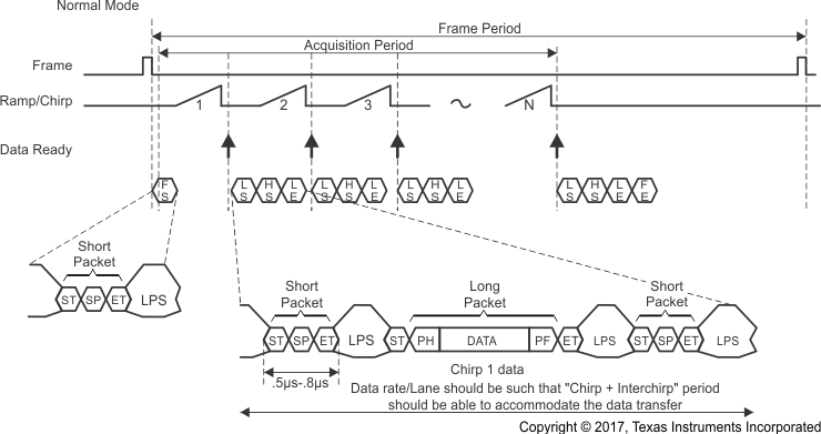
The AM273x device uses MIPI D-PHY / CSI2-based format to receive the raw A2D samples from an external radar transceiver. This is shown in Figure 7-1.
- Supports four data lanes
- CSI-2 data rate scalable from 150 Mbps to 600 Mbps per lane
- Virtual channel based
- CRC generation

Frame Start – CSI2 VSYNC
Start Short PacketLine Start – CSI2
HSYNC Start Short PacketLine End –
CSI2 HSYNC End Short PacketFrame End
– CSi2 VSYNC End Short Packet
Figure 7-1 CSI-2 Transmission FormatThe data payload is constructed with the following three types of information:
- Chirp profile information
- The actual chirp number
- A2D data corresponding to chirps of all four channels
- Interleaved fashion
- Chirp quality data (configurable)
The payload is then split across the four physical data lanes and transmitted to the receiving D-PHY. The data packet packing format is shown in Figure 7-2.
 Figure 7-2 Data Packet Packing Format for 12-Bit Complex Configuration