JAJSNL7B December 2021 – December 2023 AM2732 , AM2732-Q1
PRODUCTION DATA
- 1
- 1 特長
- 2 アプリケーション
- 3 概要
- 4 Device Comparison
-
5 Terminal Configuration and Functions
- 5.1 Pin Diagram
- 5.2 Pin Attributes (AM273x ZCE, NZN Packages)
- 5.3
Signal Descriptions
- 5.3.1 ADC Signal Descriptions
- 5.3.2 CPTS Signal Descriptions
- 5.3.3 CSI 2.0 Signal Descriptions
- 5.3.4 DMM Signal Descriptions
- 5.3.5 ECAP Signal Descriptions
- 5.3.6 EPWM Signal Descriptions
- 5.3.7 GPIO Signal Descriptions
- 5.3.8 I2C Signal Descriptions
- 5.3.9 Clock Signal Descriptions
- 5.3.10 JTAG Signal Descriptions
- 5.3.11 LVDS Signal Descriptions
- 5.3.12 MCAN Signal Descriptions
- 5.3.13 MCASP Signal Descriptions
- 5.3.14 Ethernet Signal Descriptions
- 5.3.15 GPIO Signal Descriptions
- 5.3.16 Power Supply Signal Descriptions
- 5.3.17 QSPI Signal Descriptions
- 5.3.18 Reserverd Signal Descriptions
- 5.3.19 UART Signal Descriptions
- 5.3.20 SPI Signal Descriptions
- 5.3.21 System Signal Descriptions
- 5.3.22 Trace Signal Descriptions
- 5.4 Pin Connectivity Requirements
-
6 Specifications
- 6.1 Absolute Maximum Ratings
- 6.2 ESD Ratings - Automotive
- 6.3 Power-On Hours (POH)
- 6.4 Recommended Operating Conditions
- 6.5 Operating Performance Points
- 6.6 Power Supply Specifications
- 6.7 I/O Buffer Type and Voltage Rail Dependency
- 6.8 CPU Specifications
- 6.9 Thermal Resistance Characteristics for nFBGA Package [ZCE285A]
- 6.10 Thermal Resistance Characteristics for nFBGA Package [NZN225A]
- 6.11 Power Consumption Summary
- 6.12
Timing and Switching Characteristics
- 6.12.1 Power Supply Sequencing and Reset Timing
- 6.12.2 Clock Specifications
- 6.12.3
Peripheral Information
- 6.12.3.1 QSPI Flash Memory Peripheral
- 6.12.3.2
MIBSPI
Peripheral
- 6.12.3.2.1 SPI Timing Conditions
- 6.12.3.2.2 SPI Master Mode Timing and Switching Parameters (CLOCK PHASE = 0, SPICLK = output, SPISIMO = output, and SPISOMI = input)
- 6.12.3.2.3 SPI Master Mode Timing and Switching Parameters (CLOCK PHASE = 1, SPICLK = output, SPISIMO = output, and SPISOMI = input)
- 6.12.3.2.4 SPI Slave Mode Timing and Switching Parameters (SPICLK = input, SPISIMO = input, and SPISOMI = output)
- 6.12.3.3
Ethernet Switch (RGMII/RMII/MII)
Peripheral
- 6.12.3.3.1 RGMII/GMII/MII Timing Conditions
- 6.12.3.3.2 RGMII Transmit Clock Switching Characteristics
- 6.12.3.3.3 RGMII Transmit Data and Control Switching Characteristics
- 6.12.3.3.4 RGMII Recieve Clock Timing Requirements
- 6.12.3.3.5 RGMII Recieve Data and Control Timing Requirements
- 6.12.3.3.6 RMII Transmit Clock Switching Characteristics
- 6.12.3.3.7 RMII Transmit Data and Control Switching Characteristics
- 6.12.3.3.8 RMII Receive Clock Timing Requirements
- 6.12.3.3.9 RMII Receive Data and Control Timing Requirements
- 6.12.3.3.10 MII Transmit Switching Characteristics
- 6.12.3.3.11 MII Receive Clock Timing Requirements
- 6.12.3.3.12 MII Receive Timing Requirements
- 6.12.3.3.13 MII Transmit Clock Timing Requirements
- 6.12.3.3.14 MDIO Interface Timings
- 6.12.3.4 LVDS/Aurora Instrumentation and Measurement Peripheral
- 6.12.3.5 UART Peripheral
- 6.12.3.6 I2C Protocol Definition
- 6.12.3.7 Controller Area Network - Flexible Data-Rate (CAN-FD)
- 6.12.3.8 CSI-2 Peripheral
- 6.12.3.9 General Purpose ADC (GPADC)
- 6.12.3.10 Enhanced Pulse-Width Modulator (ePWM)
- 6.12.3.11 Enhanced Capture (eCAP)
- 6.12.3.12 General-Purpose Input/Output
- 6.12.4 Emulation and Debug
- 7 Detailed Description
- 8 Applications, Implementation, and Layout
- 9 Device and Documentation Support
- 10Revision History
- 11Mechanical, Packaging, and Orderable Information
パッケージ・オプション
デバイスごとのパッケージ図は、PDF版データシートをご参照ください。
メカニカル・データ(パッケージ|ピン)
- NZN|225
- ZCE|285
サーマルパッド・メカニカル・データ
発注情報
6.12.1 Power Supply Sequencing and Reset Timing
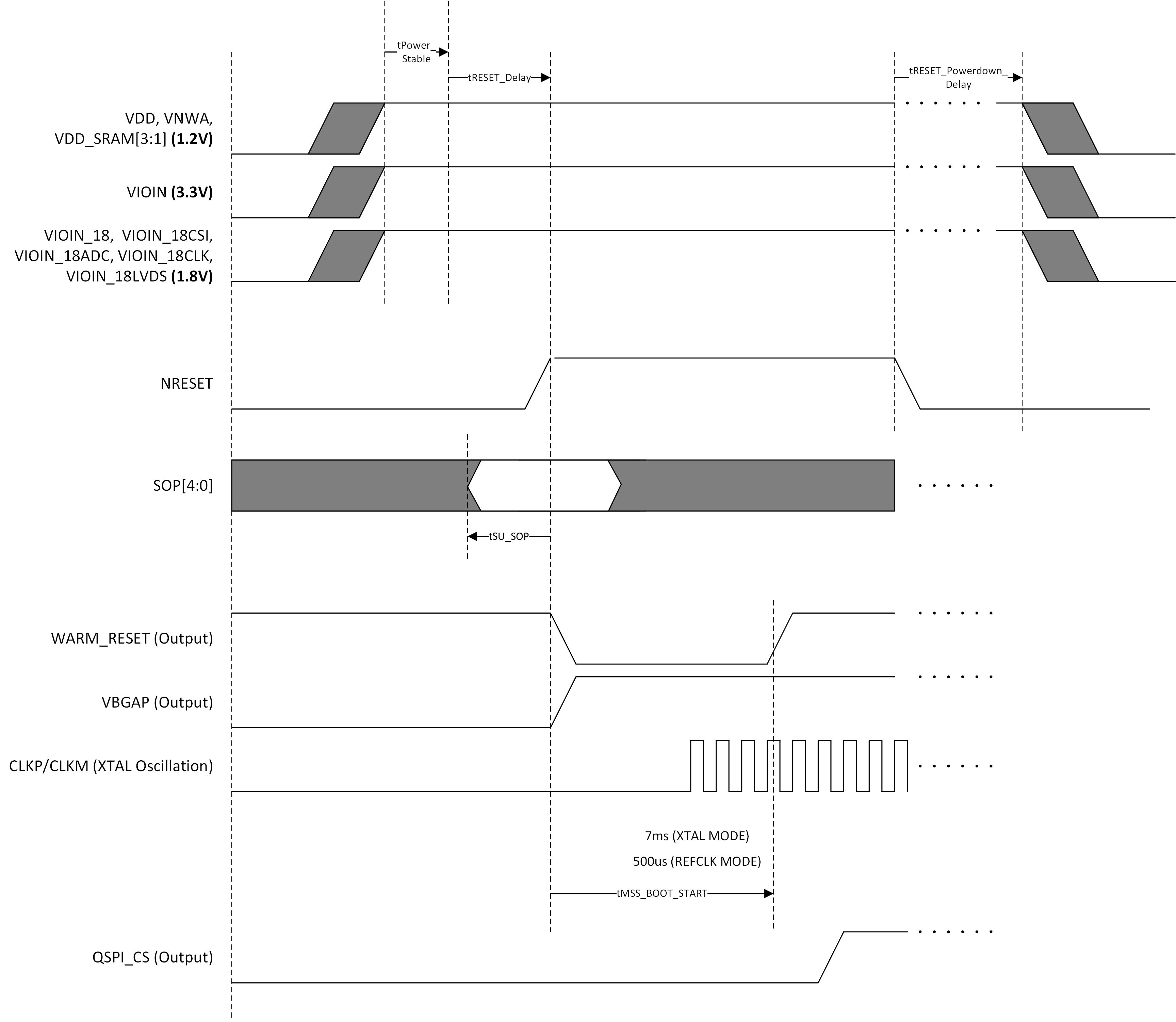
The AM273x device expects all external voltage rails and SOP boot mode select lines to be stable before NRESET is de-asserted (brought from VSS level to VIOIN level). Likewise external voltage rails should only be powered down after NRESET is asserted (brought from VIOIN level to VSS level).Figure 6-1 describes the device wake-up and power-down sequence.
 Figure 6-1 Device Wake-up and Power-Down
Sequence
Figure 6-1 Device Wake-up and Power-Down
SequenceTable 6-10 lists the timing values shown in Figure 6-1.
| NAME | DESCRIPTION | MIN | TYP | MAX | UNIT |
|---|---|---|---|---|---|
| tPOWER_STABLE |
Settling time after initial power supply turn-on after which device power nets are at valid, recommended operating conditions. NRESET should not be de-asserted (brought from GND to VIOIN level) before all power pins are at recommended operating point. See Recommended Operating Conditions for recommended operating conditions of all device power pins. |
0 | ms | ||
| tRESET_DELAY |
Delay after device power nets are at valid, nominal values, when NRESET can be brought from VSS to VIOIN level. NRESET can be brought from VSS to VIOIN level anytime after power supplies are at recommended operating conditions. |
0 | ms | ||
| tSU_SOP |
Setup time for SOP signals to be sampled by the rising edge of NRESET. Device is ready to sample SOP pin states anytime after power supplies are at recommended operating conditions. |
0 | ms | ||
| tMSS_BOOT_START |
Typical delay after NRESET rising edge before boot ROM to begins MSS code execution. Value depends on whether device is operating directly from a crystal source or oscillator (REFCLK) source. Faster startup possible with the oscillator mode. |
0.5 | 7.0 | ms | |
| tRESET_POWER_DELAY |
During power off events, delay after NRESET is brought from VIOIN to VSS level to when power pins can be powered off. Device power pins can be powered off anytime after NRESET is brought to VSS level. |
0 | ms |