SPRSPB0 December 2024 AM2754-Q1
ADVANCE INFORMATION
- 1
- 1 Features
- 2 Applications
- 3 Description
- 4 Device Comparison
-
5 Terminal Configuration and Functions
- 5.1 Pin Diagram
- 5.2 Pin Attributes
- 5.3
Signal Descriptions
- 15
- 5.3.1 ADC
- 5.3.2 Audio Clock References
- 5.3.3 CPSW
- 5.3.4 CPTS
- 5.3.5 ECAP
- 5.3.6 Emulation and Debug
- 5.3.7 EPWM
- 5.3.8 GPIO
- 5.3.9 HYPERBUS
- 5.3.10 I2C
- 5.3.11 MCAN
- 5.3.12 MCASP
- 5.3.13 MLB
- 5.3.14 MMC
- 5.3.15 OSPI
- 5.3.16 Power Supply
- 5.3.17 Reserved
- 5.3.18 System and Miscellaneous
- 5.3.19 SPI
- 5.3.20 TIMER
- 5.3.21 UART
- 5.3.22 USB
- Pin Connectivity Requirements
-
6 Specifications
- 6.1 Absolute Maximum Ratings
- 6.2 Electrostatic Discharge (ESD) for AEC - Q100 devices
- 6.3 Electrostatic Discharge (ESD) for non AEC - Q100 devices
- 6.4 Power-On Hours (POH) Summary
- 6.5 Automotive Temperature Profile
- 6.6 Recommended Operating Conditions
- 6.7 Operating Performance Points
- 6.8
Electrical
Characteristics
- 6.8.1 I2C Open-Drain and Fail-Safe (I2C OD FS) Electrical Characteristics
- 6.8.2 Fail-Safe Reset (FS RESET) Electrical Characteristics
- 6.8.3 High-Frequency Oscillators (MCU_OSC0 and OSC1) Electrical Characteristics
- 6.8.4 Low-Frequency Oscillator (WKUP_LFOSC0) Electrical Characteristics
- 6.8.5 SDIO Electrical Characteristics
- 6.8.6 Analog-to-Digital Converter (ADC)
- 6.8.7 LVCMOS Electrical Characteristics
- 6.8.8 USB2PHY Electrical Characteristics
- 6.9 VPP Specifications for One-Time Programmable (OTP) eFuses
- 6.10 Thermal Resistance Characteristics
- 6.11
Timing and Switching Characteristics
- 6.11.1 Timing Parameters and Information
- 6.11.2 Power Supply Requirements
- 6.11.3 System Timing
- 6.11.4
Clock Specifications
- 6.11.4.1 Input Clocks / Oscillators
- 6.11.4.2 Recommended System Precautions for Clock and Control Signal Transitions
- 6.11.5
Peripherals
- 6.11.5.1 ATL
- 6.11.5.2
CPSW3G
- 6.11.5.2.1 CPSW3G MDIO Timing
- 6.11.5.2.2 CPSW3G RMII Timing
- 6.11.5.2.3
CPSW3G RGMII Timing
- CPSW3G RGMII Timing Conditions
- CPSW3G RGMII[x]_RCLK Timing Requirements - RGMII Mode
- CPSW3G RGMII[x]_RD[3:0], and RGMII[x]_RCTL Timing Requirements - RGMII Mode
- 200
- CPSW3G RGMII[x]_TCLK Switching Characteristics - RGMII Mode
- CPSW3G RGMII[x]_TD[3:0], and RGMII[x]_TCTL Switching Characteristics - RGMII Mode
- 203
- 6.11.5.3 ECAP
- 6.11.5.4 Emulation and Debug
- 6.11.5.5 EPWM
- 6.11.5.6 GPIO
- 6.11.5.7 HyperBus
- 6.11.5.8 I2C
- 6.11.5.9 MCAN
- 6.11.5.10 MCASP
- 6.11.5.11 MCSPI
- 6.11.5.12 MLB
- 6.11.5.13
MMCSD
- 6.11.5.13.1
MMC0 - eMMC/SDIO Interface
- MMC Timing Conditions
- MMC Timing Requirements - 3.3V Legacy SDR Mode
- 267
- MMC Switching Characteristics - 3.3V Legacy SDR Mode
- 269
- MMC Timing Requirements - 3.3V High Speed SDR Mode
- 271
- MMC Switching Characteristics - 3.3V High Speed SDR Mode
- 273
- MMC Timing Requirements - 1.8V Legacy SDR, UHS-I SDR12 Mode
- 275
- MMC Switching Characteristics - 1.8V Legacy SDR, UHS-I SDR12 Mode
- 277
- MMC Timing Requirements - 1.8V High Speed SDR, UHS-I SDR25 Mode
- 279
- MMC Switching Characteristics - 1.8V High Speed SDR, UHS-I SDR25 Mode
- 281
- MMC Switching Characteristics - UHS-I SDR50 Mode
- 283
- MMC Switching Characteristics - UHS-I DDR50 Mode
- 285
- MMC Switching Characteristics - HS200 Mode
- 287
- 6.11.5.13.1
MMC0 - eMMC/SDIO Interface
- 6.11.5.14 OSPI
- 6.11.5.15 Timers
- 6.11.5.16 UART
- 6.11.5.17 USB
- 7 Detailed Description
- 8 Applications, Implementation, and Layout
- 9 Device and Documentation Support
- 10Revision History
- 11Mechanical, Packaging, and Orderable Information
6.11.4.1.1.4 Shunt Capacitance
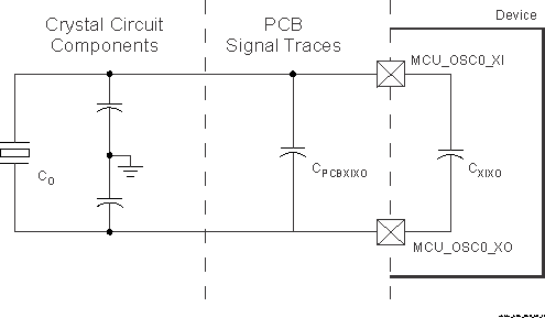
The crystal circuit must also be designed such that it does not exceed the maximum shunt capacitance for MCU_OSC0 operating conditions defined in HFOSC (MCU_OSC0 and OSC1) Crystal Circuit Requirements. Shunt capacitance, Cshunt, of the crystal circuit is a combination of crystal shunt capacitance and parasitic contributions. PCB signal traces which connect crystal circuit components to MCU_OSC0 have mutual parasitic capacitance to each other, CPCBXIXO, where the PCB designer should be able to extract mutual parasitic capacitance between these signal traces. The device package also has mutual parasitic capacitance, CXIXO, where this mutual parasitic capacitance value is defined in HFOSC (MCU_OSC0 and OSC1) Switching Characteristics - Crystal Mode.
PCB routing should be designed to minimize mutual capacitance between XI and XO signal traces. This is typically done by keeping signal traces short and not routing them in close proximity. Mutual capacitance can also be minimized by placing a ground trace between these signals when the layout requires them to be routed in close proximity. It is important to minimize the mutual capacitance on the PCB to provide as much margin as possible when selecting a crystal.
 Figure 6-16 Shunt Capacitance
A crystal should be chosen such that the below equation is satisfied. CO in the equation is the maximum shunt capacitance specified by the crystal manufacturer.
Cshunt ≥ CO + CPCBXIXO + CXIXO
For example, the equation would be satisfied when the crystal being used is 25 MHz with an ESR = 30 Ω, CPCBXIXO = 0.04 pF, CXIXO = 0.01 pF, and shunt capacitance of the crystal is less than or equal to 6.95 pF.