SPRSPB0 December 2024 AM2754-Q1
ADVANCE INFORMATION
- 1
- 1 Features
- 2 Applications
- 3 Description
- 4 Device Comparison
-
5 Terminal Configuration and Functions
- 5.1 Pin Diagram
- 5.2 Pin Attributes
- 5.3
Signal Descriptions
- 15
- 5.3.1 ADC
- 5.3.2 Audio Clock References
- 5.3.3 CPSW
- 5.3.4 CPTS
- 5.3.5 ECAP
- 5.3.6 Emulation and Debug
- 5.3.7 EPWM
- 5.3.8 GPIO
- 5.3.9 HYPERBUS
- 5.3.10 I2C
- 5.3.11 MCAN
- 5.3.12 MCASP
- 5.3.13 MLB
- 5.3.14 MMC
- 5.3.15 OSPI
- 5.3.16 Power Supply
- 5.3.17 Reserved
- 5.3.18 System and Miscellaneous
- 5.3.19 SPI
- 5.3.20 TIMER
- 5.3.21 UART
- 5.3.22 USB
- Pin Connectivity Requirements
-
6 Specifications
- 6.1 Absolute Maximum Ratings
- 6.2 Electrostatic Discharge (ESD) for AEC - Q100 devices
- 6.3 Electrostatic Discharge (ESD) for non AEC - Q100 devices
- 6.4 Power-On Hours (POH) Summary
- 6.5 Automotive Temperature Profile
- 6.6 Recommended Operating Conditions
- 6.7 Operating Performance Points
- 6.8
Electrical
Characteristics
- 6.8.1 I2C Open-Drain and Fail-Safe (I2C OD FS) Electrical Characteristics
- 6.8.2 Fail-Safe Reset (FS RESET) Electrical Characteristics
- 6.8.3 High-Frequency Oscillators (MCU_OSC0 and OSC1) Electrical Characteristics
- 6.8.4 Low-Frequency Oscillator (WKUP_LFOSC0) Electrical Characteristics
- 6.8.5 SDIO Electrical Characteristics
- 6.8.6 Analog-to-Digital Converter (ADC)
- 6.8.7 LVCMOS Electrical Characteristics
- 6.8.8 USB2PHY Electrical Characteristics
- 6.9 VPP Specifications for One-Time Programmable (OTP) eFuses
- 6.10 Thermal Resistance Characteristics
- 6.11
Timing and Switching Characteristics
- 6.11.1 Timing Parameters and Information
- 6.11.2 Power Supply Requirements
- 6.11.3 System Timing
- 6.11.4
Clock Specifications
- 6.11.4.1 Input Clocks / Oscillators
- 6.11.4.2 Recommended System Precautions for Clock and Control Signal Transitions
- 6.11.5
Peripherals
- 6.11.5.1 ATL
- 6.11.5.2
CPSW3G
- 6.11.5.2.1 CPSW3G MDIO Timing
- 6.11.5.2.2 CPSW3G RMII Timing
- 6.11.5.2.3
CPSW3G RGMII Timing
- CPSW3G RGMII Timing Conditions
- CPSW3G RGMII[x]_RCLK Timing Requirements - RGMII Mode
- CPSW3G RGMII[x]_RD[3:0], and RGMII[x]_RCTL Timing Requirements - RGMII Mode
- 200
- CPSW3G RGMII[x]_TCLK Switching Characteristics - RGMII Mode
- CPSW3G RGMII[x]_TD[3:0], and RGMII[x]_TCTL Switching Characteristics - RGMII Mode
- 203
- 6.11.5.3 ECAP
- 6.11.5.4 Emulation and Debug
- 6.11.5.5 EPWM
- 6.11.5.6 GPIO
- 6.11.5.7 HyperBus
- 6.11.5.8 I2C
- 6.11.5.9 MCAN
- 6.11.5.10 MCASP
- 6.11.5.11 MCSPI
- 6.11.5.12 MLB
- 6.11.5.13
MMCSD
- 6.11.5.13.1
MMC0 - eMMC/SDIO Interface
- MMC Timing Conditions
- MMC Timing Requirements - 3.3V Legacy SDR Mode
- 267
- MMC Switching Characteristics - 3.3V Legacy SDR Mode
- 269
- MMC Timing Requirements - 3.3V High Speed SDR Mode
- 271
- MMC Switching Characteristics - 3.3V High Speed SDR Mode
- 273
- MMC Timing Requirements - 1.8V Legacy SDR, UHS-I SDR12 Mode
- 275
- MMC Switching Characteristics - 1.8V Legacy SDR, UHS-I SDR12 Mode
- 277
- MMC Timing Requirements - 1.8V High Speed SDR, UHS-I SDR25 Mode
- 279
- MMC Switching Characteristics - 1.8V High Speed SDR, UHS-I SDR25 Mode
- 281
- MMC Switching Characteristics - UHS-I SDR50 Mode
- 283
- MMC Switching Characteristics - UHS-I DDR50 Mode
- 285
- MMC Switching Characteristics - HS200 Mode
- 287
- 6.11.5.13.1
MMC0 - eMMC/SDIO Interface
- 6.11.5.14 OSPI
- 6.11.5.15 Timers
- 6.11.5.16 UART
- 6.11.5.17 USB
- 7 Detailed Description
- 8 Applications, Implementation, and Layout
- 9 Device and Documentation Support
- 10Revision History
- 11Mechanical, Packaging, and Orderable Information
8.2.1.2 External Board Loopback
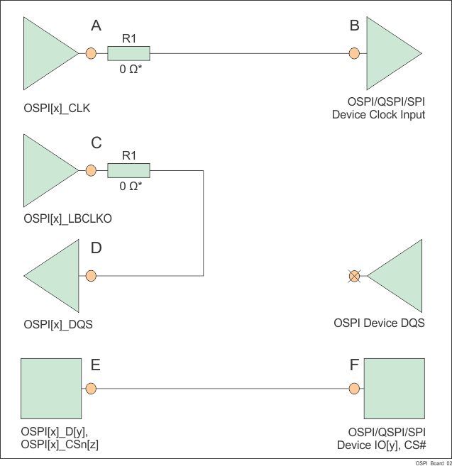
- The OSPI[x]_CLK output pin must be connected to the CLK input pin of the attached OSPI/QSPI/SPI device
- The OSPI[x]_LBCLKO output pin must be looped back to the OSPI[x]_DQS input pin
- The signal propagation delay of the OSPI[x]_LBCLKO pin to the OSPI[x]_DQS pin (C to D) must be approximately twice the propagation delay of the OSPI[x]_CLK pin to the attached OSPI/QSPI/SPI device CLK pin (A to B)
- The signal propagation delay of each OSPI[x]_D[y] and OSPI[x]_CSn[z] pin to the corresponding attached OSPI/QSPI/SPI device data and control pin (E to F, or F to E) must be approximately equal to the signal propagation delay from the OSPI[x]_CLK pin to the attached OSPI/QSPI/SPI device CLK pin (A to B)
- 50 Ω PCB routing is recommended along with series terminations, as shown in Figure 8-2
- Propagation delays and matching:
- (C to D) = 2 x ((A to B) ± 30 ps), see the exception note below.
- (E to F, or F to E) = ((A to B) ± 60 ps)
Note:
The External Board Loopback hold time requirement (defined by parameter number O16 in the OSPI0 Timing Requirements - PHY DDR Mode section) may be larger than the hold time provided by a typical OSPI/QSPI/SPI device. In this case, the propagation delay of OPSI[x]_LBCLKO pin to the OSPI[x]_DQS pin (C to D) can be reduced to provide additional hold time.

* 0 Ω resistor
(R1), located as close as possible to the OSPI[x]_CLK and OSPI[x]_LBCLKO pins,
is a placeholder for fine tuning, if needed.
Figure 8-2 OSPI
Connectivity Schematic for External Board Loopback