SPRS982H December 2016 – December 2019 AM5746 , AM5748 , AM5749
PRODUCTION DATA.
- 1Device Overview
- 2Revision History
- 3Device Comparison
-
4Terminal Configuration and Functions
- 4.1 Pin Diagram
- 4.2 Pin Attributes
- 4.3
Signal Descriptions
- 4.3.1 VIP
- 4.3.2 DSS
- 4.3.3 HDMI
- 4.3.4 EMIF
- 4.3.5 GPMC
- 4.3.6 Timer
- 4.3.7 I2C
- 4.3.8 HDQ1W
- 4.3.9 UART
- 4.3.10 McSPI
- 4.3.11 QSPI
- 4.3.12 McASP
- 4.3.13 USB
- 4.3.14 SATA
- 4.3.15 PCIe
- 4.3.16 DCAN and MCAN
- 4.3.17 GMAC_SW
- 4.3.18 MLB
- 4.3.19 eMMC/SD/SDIO
- 4.3.20 GPIO
- 4.3.21 KBD
- 4.3.22 PWM
- 4.3.23 PRU-ICSS
- 4.3.24 Test Interfaces
- 4.3.25 System and Miscellaneous
- 4.4 Pin Multiplexing
- 4.5 Connections for Unused Pins
-
5Specifications
- 5.1 Absolute Maximum Ratings
- 5.2 ESD Ratings
- 5.3 Power-On Hours (POH) Limits
- 5.4 Recommended Operating Conditions
- 5.5 Operating Performance Points
- 5.6 Power Consumption Summary
- 5.7
Electrical Characteristics
- Table 5-7 LVCMOS DDR DC Electrical Characteristics
- Table 5-8 Dual Voltage LVCMOS I2C DC Electrical Characteristics
- Table 5-9 IQ1833 Buffers DC Electrical Characteristics
- Table 5-10 IHHV1833 Buffers DC Electrical Characteristics
- Table 5-11 LVCMOS OSC Buffers DC Electrical Characteristics
- Table 5-12 BC1833IHHV Buffers DC Electrical Characteristics
- Table 5-13 Dual Voltage SDIO1833 DC Electrical Characteristics
- Table 5-14 Dual Voltage LVCMOS DC Electrical Characteristics
- 5.7.1 HDMIPHY DC Electrical Characteristics
- 5.7.2 USBPHY DC Electrical Characteristics
- 5.7.3 SATAPHY DC Electrical Characteristics
- 5.7.4 PCIEPHY DC Electrical Characteristics
- 5.8 VPP Specifications for One-Time Programmable (OTP) eFuses
- 5.9 Thermal Characteristics
- 5.10
Timing Requirements and Switching Characteristics
- 5.10.1 Timing Parameters and Information
- 5.10.2 Interface Clock Specifications
- 5.10.3 Power Supply Sequences
- 5.10.4 Clock Specifications
- 5.10.5 Recommended Clock and Control Signal Transition Behavior
- 5.10.6
Peripherals
- 5.10.6.1 Timing Test Conditions
- 5.10.6.2 Virtual and Manual I/O Timing Modes
- 5.10.6.3 VIP
- 5.10.6.4 DSS
- 5.10.6.5 HDMI
- 5.10.6.6 EMIF
- 5.10.6.7 GPMC
- 5.10.6.8 I2C
- 5.10.6.9 HDQ1W
- 5.10.6.10 UART
- 5.10.6.11 McSPI
- 5.10.6.12 QSPI
- 5.10.6.13
McASP
- Table 5-80 Timing Requirements for McASP1
- Table 5-81 Timing Requirements for McASP2
- Table 5-82 Timing Requirements for McASP3/4/5/6/7/8
- Table 5-83 Switching Characteristics Over Recommended Operating Conditions for McASP1
- Table 5-84 Switching Characteristics Over Recommended Operating Conditions for McASP2
- Table 5-85 Switching Characteristics Over Recommended Operating Conditions for McASP3/4/5/6/7/8
- 5.10.6.14 USB
- 5.10.6.15 SATA
- 5.10.6.16 PCIe
- 5.10.6.17 CAN
- 5.10.6.18
GMAC_SW
- 5.10.6.18.1
GMAC MII Timings
- Table 5-99 Timing Requirements for miin_rxclk - MII Operation
- Table 5-100 Timing Requirements for miin_txclk - MII Operation
- Table 5-101 Timing Requirements for GMAC MIIn Receive 10/100 Mbit/s
- Table 5-102 Switching Characteristics Over Recommended Operating Conditions for GMAC MIIn Transmit 10/100 Mbits/s
- 5.10.6.18.2 GMAC MDIO Interface Timings
- 5.10.6.18.3
GMAC RMII Timings
- Table 5-107 Timing Requirements for GMAC REF_CLK - RMII Operation
- Table 5-108 Timing Requirements for GMAC RMIIn Receive
- Table 5-109 Switching Characteristics Over Recommended Operating Conditions for GMAC REF_CLK - RMII Operation
- Table 5-110 Switching Characteristics Over Recommended Operating Conditions for GMAC RMIIn Transmit 10/100 Mbits/s
- 5.10.6.18.4
GMAC RGMII Timings
- Table 5-114 Timing Requirements for rgmiin_rxc - RGMIIn Operation
- Table 5-115 Timing Requirements for GMAC RGMIIn Input Receive for 10/100/1000 Mbps
- Table 5-116 Switching Characteristics Over Recommended Operating Conditions for rgmiin_txctl - RGMIIn Operation for 10/100/1000 Mbit/s
- Table 5-117 Switching Characteristics for GMAC RGMIIn Output Transmit for 10/100/1000 Mbps
- 5.10.6.18.1
GMAC MII Timings
- 5.10.6.19
eMMC/SD/SDIO
- 5.10.6.19.1
MMC1—SD Card Interface
- 5.10.6.19.1.1 Default speed, 4-bit data, SDR, half-cycle
- 5.10.6.19.1.2 High speed, 4-bit data, SDR, half-cycle
- 5.10.6.19.1.3 SDR12, 4-bit data, half-cycle
- 5.10.6.19.1.4 SDR25, 4-bit data, half-cycle
- 5.10.6.19.1.5 UHS-I SDR50, 4-bit data, half-cycle
- 5.10.6.19.1.6 UHS-I SDR104, 4-bit data, half-cycle
- 5.10.6.19.1.7 UHS-I DDR50, 4-bit data
- 5.10.6.19.2 MMC2 — eMMC
- 5.10.6.19.3 MMC3 and MMC4—SDIO/SD
- 5.10.6.19.1
MMC1—SD Card Interface
- 5.10.6.20
PRU-ICSS
- 5.10.6.20.1 Programmable Real-Time Unit (PRU-ICSS PRU)
- 5.10.6.20.2
PRU-ICSS EtherCAT (PRU-ICSS ECAT)
- 5.10.6.20.2.1
PRU-ICSS ECAT Electrical Data and Timing
- Table 5-174 PRU-ICSS ECAT Timing Requirements – Input Validated With LATCH_IN
- Table 5-175 PRU-ICSS ECAT Timing Requirements – Input Validated With SYNCx
- Table 5-176 PRU-ICSS ECAT Timing Requirements – Input Validated With Start of Frame (SOF)
- Table 5-177 PRU-ICSS ECAT Timing Requirements - LATCHx_IN
- Table 5-178 PRU-ICSS ECAT Switching Requirements - Digital IOs
- 5.10.6.20.2.1
PRU-ICSS ECAT Electrical Data and Timing
- 5.10.6.20.3 PRU-ICSS MII_RT and Switch
- 5.10.6.20.4 PRU-ICSS Universal Asynchronous Receiver Transmitter (PRU-ICSS UART)
- 5.10.6.20.5 PRU-ICSS IOSETs
- 5.10.6.20.6 PRU-ICSS Manual Functional Mapping
- 5.10.6.21 System and Miscellaneous interfaces
- 5.10.7
Emulation and Debug Subsystem
- 5.10.7.1
JTAG
- 5.10.7.1.1
JTAG Electrical Data/Timing
- Table 5-210 Timing Requirements for IEEE 1149.1 JTAG
- Table 5-211 Switching Characteristics Over Recommended Operating Conditions for IEEE 1149.1 JTAG
- Table 5-212 Timing Requirements for IEEE 1149.1 JTAG With RTCK
- Table 5-213 Switching Characteristics Over Recommended Operating Conditions for IEEE 1149.1 JTAG With RTCK
- 5.10.7.1.1
JTAG Electrical Data/Timing
- 5.10.7.2 TPIU
- 5.10.7.1
JTAG
-
6Detailed Description
- 6.1 Overview
- 6.2 Processor Subsystems
- 6.3 Accelerators and Coprocessors
- 6.4
Other Subsystems
- 6.4.1 Memory Subsystem
- 6.4.2 EDMA
- 6.4.3 Peripherals
- 6.4.4 On-Chip Debug
- 6.5 Identification
- 6.6 Boot Modes
-
7Applications, Implementation, and Layout
- 7.1 Power Supply Mapping
- 7.2
DDR3 Board Design and Layout Guidelines
- 7.2.1 DDR3 General Board Layout Guidelines
- 7.2.2
DDR3 Board Design and Layout Guidelines
- 7.2.2.1 Board Designs
- 7.2.2.2 DDR3 EMIFs
- 7.2.2.3 DDR3 Device Combinations
- 7.2.2.4 DDR3 Interface Schematic
- 7.2.2.5 Compatible JEDEC DDR3 Devices
- 7.2.2.6 PCB Stackup
- 7.2.2.7 Placement
- 7.2.2.8 DDR3 Keepout Region
- 7.2.2.9 Bulk Bypass Capacitors
- 7.2.2.10 High Speed Bypass Capacitors
- 7.2.2.11 Net Classes
- 7.2.2.12 DDR3 Signal Termination
- 7.2.2.13 VREF_DDR Routing
- 7.2.2.14 VTT
- 7.2.2.15 CK and ADDR_CTRL Topologies and Routing Definition
- 7.2.2.16 Data Topologies and Routing Definition
- 7.2.2.17 Routing Specification
- 7.3 High Speed Differential Signal Routing Guidance
- 7.4 Power Distribution Network Implementation Guidance
- 7.5 Thermal Solution Guidance
- 7.6 Single-Ended Interfaces
- 7.7 LJCB_REFN/P Connections
- 7.8 Clock Routing Guidelines
- 8Device and Documentation Support
- 9Mechanical, Packaging, and Orderable Information
パッケージ・オプション
デバイスごとのパッケージ図は、PDF版データシートをご参照ください。
メカニカル・データ(パッケージ|ピン)
- ABZ|760
サーマルパッド・メカニカル・データ
発注情報
5.10.3 Power Supply Sequences
This section describes the power-up and power-down sequence required to ensure proper device operation. The power supply names described in this section comprise a superset of a family of compatible devices. Some members of this family will not include a subset of these power supplies and their associated device modules. Refer to the Section 4.2, Pin Attributes of the Section 4, Terminal Configuration and Functions to determine which power supplies are applicable.
NOTE
RTC-only mode is not a supported feature.
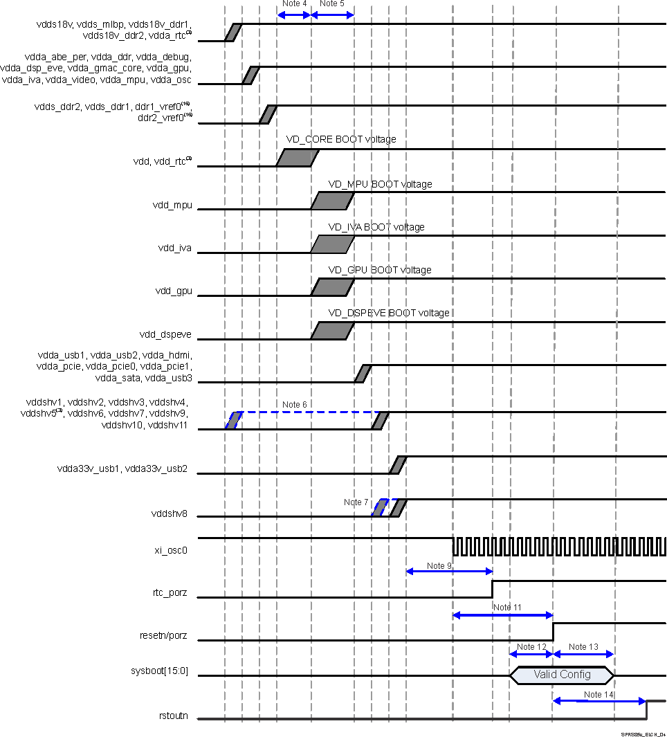
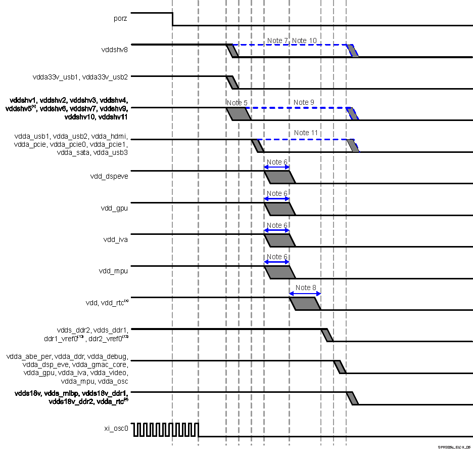
Figure 5-5 and Figure 5-6 describe the device power sequencing when RTC-mode is NOT used.
 Figure 5-5 Power-Up Sequencing(2)
 - Grey shaded areas are windows where it is valid to ramp the voltage rail.
- Blue dashed lines are not valid windows but show alternate ramp possibilities based on the associated note.
- If RTC-only mode is not used then the following combinations are approved:
- vdda_rtc can be combined with vdds18v
- vdd_rtc can be combined with vdd
- vddshv5 can be combined with other 1.8 V or 3.3 V vddshvn rails.
If combinations listed above are not followed then sequencing for these 3 voltage rails should follow the RTC mode timing requirements. When using RTC mode timing:
- vdda_rtc rises coincident with, or before, the 1.8 V interface supplies (such as vdds18v).
- vdd_rtc rises coincident with vdd, or it may rise earlier. If rising earlier, it must rise after the 1.8 V interface supplies.
- vddshv5 rises coincident with the other vddshvn rails (of the same voltage) or it can rise about the same time as the 1.8 V PHY supplies (such as vdd_usb1).
- vdd must ramp before or at the same time as vdd_mpu, vdd_gpu, vdd_dspeve and vdd_iva.
- vdd_mpu, vdd_gpu, vdd_dspeve, vdd_iva can be ramped at the same time or can be staggered.
- If any of the vddshv[1-7,9-11] rails (not including vddshv8) are used as 1.8 V only, then these rails can be combined with vdds18v.
- vddshv8 is separated out to show support for dual voltage. If single voltage is used then vddshv8 can be combined with other vddshvn rails but vddshv8 must ramp after vdd.
- vdds and vdda rails must not be combined together, with the one exception of vdda_rtc when RTC-mode is not supported.
- Pulse duration: rtc_porz must remain low 1 ms after vdda_rtc, vddshv5, and vdd_rtc are ramped and stable.
- The FUNC_32K_CLK source must be stable and at a valid frequency 1ms prior to deasserting rtc_porz high.
- porz must remain asserted low until all of the following conditions are met:
- All device supply rails reach stable operational levels.
- xi_osc0 is stable and at a valid frequency.
- Minimum of 12P after both of the above conditions are met, where P = 1 / (SYS_CLK1/610), units in ns.
- Setup time: sysboot[15:0] pins must be valid 2P(15) before porz is de-asserted high.
- Hold time: sysboot[15:0] pins must be valid 15P(15) after porz is de-asserted high.
- rstoutn will be asserted low when porz is low, and de-asserted following an internal 2ms delay. rstoutn is only valid after vddshv3 reaches an operational level. If used as a peripheral component reset, it should be AND gated with porz to avoid possible reset glitches during power up.
- P = 1 / (SYS_CLK1 / 610) µs, where SYS_CLK1 is in MHz.
- ddr1_vref0 / ddr2_vref0 may rise coincident with vdds_ddr1 / vdds_ddr2, respectively or at a later time. However, it must be valid before porz rising.
- Grey shaded areas are windows where it is valid to ramp the voltage rail.
- Blue dashed lines are not valid windows but show alternate ramp possibilities based on the associated note.
- xi_osc0 can be turned off anytime after porz assertion and must be turned off before vdda_osc voltage rail is shutdown.
- If RTC-mode is not used then the following combinations are approved:
- vdda_rtc can be combined with vdds18v
- vdd_rtc can be combined with vdd
- vddshv5 can be combined with other 1.8 V or 3.3 V vddshv* rails
If combinations listed above are not followed then sequencing for these 3 voltage rails should follow the RTC mode timing requirements. When using RTC mode timing:
- vdda_rtc falls coincident with, or later than, the 1.8 V interface supplies (such as vdds18v).
- vdd_rtc falls coincident with vdd, or it may fall later. If falling later, it must fall before, or coincident with, the 1.8 V interface supplies.
- vddshv5 falls coincident with the other vddshvn rails (of the same voltage) or it can fall about the same time as the 1.8 V PHY supplies (such as vdd_usb1).
- vddshv* domains supplied by 3.3 V:
- must remain greater than 2.7 V to enable Dual Voltage GPIO selector circuit operation for 100 µs min after porz is asserted low.
- must be in first group of supplies ramping down after porz has been asserted low for 100 µs min.
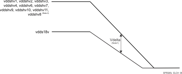
- must not exceed vdds18v by more than 2 V during ramp down, see Figure 5-7 “vdds18v versus vddshv* Discharge Relationship”.
- vdd_mpu, vdd_gpu, vdd_dspeve, vdd_iva can be ramped at the same time or can be staggered.
- vddshv8 domain:
- if SDIO operation is needed,
- must be in first group of supplies to ramp down after porz has been asserted low for 100 µs min.
- must be sourced from independent power resource that can provide dual voltage (3.3 V / 1.8 V) operation as required to be compliant to SDIO specification
- if SDIO operation is not needed,
- must be grouped and ramped down with other vddshv* domains as noted above.
- if SDIO operation is needed,
- vdd must ramp after or at the same time as vdd_mpu, vdd_gpu, vdd_dspeve and vdd_iva.
- If any of the vddshv[1-7,9-11] rails (not including vddshv8) are used as 1.8 V only, then these rails can be combined with vdds18v. vddshv[1-7,9-11] is allowed to ramp down at either of the two points shown in the timing diagram in either 1.8 V mode or in 3.3 V mode. If vddshv[1-7,9-11] ramps down at the later time in the diagram then the board design must ensure that the vddshv[1-7,9-11] rail is never higher than 2.0 V above the vdds18v rail.
- vddshv8 is separated out to show support for dual voltage. If a dedicated LDO/supply source is used for vddshv8, then vddshv8 ramp down should occur at one of the two earliest points in the timing diagram. If vddshv8 is powered by the same supply source as the other vddshv[1-7,9-11] rails, then it is allowed to ramp down at either of the last two points in the timing diagram.
- The 1.8 V vdda_* supplies can either ramp down at the earlier time period shown or can be delayed to ramp down after the core supplies coincident with the vdds18v supply as long as porz is asserted (low) during the power down sequence.
- The power down sequence shown is the most general case and is always valid. An accelerated power down sequence is also available but is only valid when porz is asserted (low). This accelerated power down sequence has been implemented in the companion PMIC that is recommended for use with this SoC. The accelerated sequence has porz go low first, then all 3.3 V supplies simultaneously second, core supplies, DDR supplies and DDR references simultaneously third and all 1.8 V supplies simultaneously last.
- ddr1_vref0 / ddr2_vref0 may fall coincident with vdds_ddr1 / vdds_ddr2, respectively or at a prior time but after porz is asserted low.
- Ramped Down is defined as reaching a voltage level of no more than 0.6 V.
Figure 5-7 describes the discharge relationship between vdds18v and vddshv* power supplies during power-down.
 Figure 5-7 vdds18v versus vddshv* Discharge Relationship
 - Vdelta MAX = 2 V
- If vddshv8 is powered by the same supply source as the other vddshv[1-7,9-11] rails.
