JAJSQZ4B March 2023 – September 2023 AM62A3 , AM62A3-Q1 , AM62A7 , AM62A7-Q1
PRODUCTION DATA
- 1
- 1 特長
- 2 アプリケーション
- 3 概要
- 4 Device Comparison
-
5 Terminal Configuration and Functions
- 5.1 Pin Diagrams
- 5.2 Pin Attributes
- 5.3
Signal Descriptions
- 14
- 5.3.1 CPSW3G
- 5.3.2 CPTS
- 5.3.3 CSI-2
- 5.3.4 DDRSS
- 5.3.5 DSS
- 5.3.6 ECAP
- 5.3.7 Emulation and Debug
- 5.3.8 EPWM
- 5.3.9 EQEP
- 5.3.10 GPIO
- 5.3.11 GPMC
- 5.3.12 I2C
- 5.3.13 MCAN
- 5.3.14 MCASP
- 5.3.15 MCSPI
- 5.3.16 MDIO
- 5.3.17 MMC
- 5.3.18 OSPI
- 5.3.19 Power Supply
- 5.3.20 Reserved
- 5.3.21 System and Miscellaneous
- 5.3.22 TIMER
- 5.3.23 UART
- 5.3.24 USB
- 5.4 Pin Connectivity Requirements
-
6 Specifications
- 6.1 Absolute Maximum Ratings
- 6.2 ESD Ratings for Devices which are not AEC - Q100 Qualified
- 6.3 ESD Ratings for AEC - Q100 Qualified Devices
- 6.4 Power-On Hours (POH)
- 6.5 Recommended Operating Conditions
- 6.6 Operating Performance Points
- 6.7 Power Consumption Summary
- 6.8
Electrical
Characteristics
- 6.8.1 I2C Open-Drain, and Fail-Safe (I2C OD FS) Electrical Characteristics
- 6.8.2 Fail-Safe Reset (FS RESET) Electrical Characteristics
- 6.8.3 High-Frequency Oscillator (HFOSC) Electrical Characteristics
- 6.8.4 Low-Frequency Oscillator (LFXOSC) Electrical Characteristics
- 6.8.5 SDIO Electrical Characteristics
- 6.8.6 LVCMOS Electrical Characteristics
- 6.8.7 CSI-2 (D-PHY) Electrical Characteristics
- 6.8.8 USB2PHY Electrical Characteristics
- 6.8.9 DDR Electrical Characteristics
- 6.9 VPP Specifications for One-Time Programmable (OTP) eFuses
- 6.10 Thermal Resistance Characteristics
- 6.11
Timing and Switching Characteristics
- 6.11.1 Timing Parameters and Information
- 6.11.2 Power Supply Requirements
- 6.11.3 System Timing
- 6.11.4
Clock Specifications
- 6.11.4.1 Input Clocks / Oscillators
- 6.11.4.2 Output Clocks
- 6.11.4.3 PLLs
- 6.11.4.4 Recommended System Precautions for Clock and Control Signal Transitions
- 6.11.5
Peripherals
- 6.11.5.1 CPSW3G
- 6.11.5.2 CPTS
- 6.11.5.3 CSI-2
- 6.11.5.4 DDRSS
- 6.11.5.5 DSS
- 6.11.5.6 ECAP
- 6.11.5.7 Emulation and Debug
- 6.11.5.8 EPWM
- 6.11.5.9 EQEP
- 6.11.5.10 GPIO
- 6.11.5.11 GPMC
- 6.11.5.12 I2C
- 6.11.5.13 MCAN
- 6.11.5.14 MCASP
- 6.11.5.15 MCSPI
- 6.11.5.16
MMCSD
- 6.11.5.16.1
MMC0 - eMMC/SD/SDIO Interface
- 6.11.5.16.1.1 Legacy SDR Mode
- 6.11.5.16.1.2 High Speed SDR Mode
- 6.11.5.16.1.3 HS200 Mode
- 6.11.5.16.1.4 Default Speed Mode
- 6.11.5.16.1.5 High Speed Mode
- 6.11.5.16.1.6 UHS–I SDR12 Mode
- 6.11.5.16.1.7 UHS–I SDR25 Mode
- 6.11.5.16.1.8 UHS–I SDR50 Mode
- 6.11.5.16.1.9 UHS–I DDR50 Mode
- 6.11.5.16.1.10 UHS–I SDR104 Mode
- 6.11.5.16.2 MMC1/MMC2 - SD/SDIO Interface
- 6.11.5.16.1
MMC0 - eMMC/SD/SDIO Interface
- 6.11.5.17 OSPI
- 6.11.5.18 Timers
- 6.11.5.19 UART
- 6.11.5.20 USB
-
7 Detailed Description
- 7.1 Overview
- 7.2 Processor Subsystems
- 7.3 Accelerators and Coprocessors
- 7.4 Other Subsystems
- 7.5
Peripherals
- 7.5.1 Gigabit Ethernet Switch (CPSW3G)
- 7.5.2 Camera Serial Interface Receiver (CSI_RX_IF)
- 7.5.3 Display Subsystem (DSS)
- 7.5.4 Enhanced Capture (ECAP)
- 7.5.5 Error Location Module (ELM)
- 7.5.6 Enhanced Pulse Width Modulation (EPWM)
- 7.5.7 Error Signaling Module (ESM)
- 7.5.8 Enhanced Quadrature Encoder Pulse (EQEP)
- 7.5.9 General-Purpose Interface (GPIO)
- 7.5.10 General-Purpose Memory Controller (GPMC)
- 7.5.11 Global Timebase Counter (GTC)
- 7.5.12 Inter-Integrated Circuit (I2C)
- 7.5.13 Modular Controller Area Network (MCAN)
- 7.5.14 Multichannel Audio Serial Port (MCASP)
- 7.5.15 Multichannel Serial Peripheral Interface (MCSPI)
- 7.5.16 Multi-Media Card Secure Digital (MMCSD)
- 7.5.17 Octal Serial Peripheral Interface (OSPI)
- 7.5.18 Timers
- 7.5.19 Universal Asynchronous Receiver/Transmitter (UART)
- 7.5.20 Universal Serial Bus Subsystem (USBSS)
-
8 Applications,
Implementation, and Layout
- 8.1 Device Connection and Layout Fundamentals
- 8.2 Peripheral- and Interface-Specific Design Information
- 8.3 Clock Routing Guidelines
- 9 Device and Documentation Support
- 10Revision History
- 11Mechanical, Packaging, and Orderable Information
パッケージ・オプション
デバイスごとのパッケージ図は、PDF版データシートをご参照ください。
メカニカル・データ(パッケージ|ピン)
- AMB|484
サーマルパッド・メカニカル・データ
発注情報
6.11.5.11.2 GPMC and NOR Flash — Asynchronous Mode
Table 6-65 and Table 6-66 present timing requirements and switching characteristics for GPMC and NOR Flash — Asynchronous Mode.
Table 6-65 GPMC and NOR Flash Timing
Requirements – Asynchronous Mode see Figure 6-51, Figure 6-52, Figure 6-53, and Figure 6-55
| NO. | PARAMETER | DESCRIPTION | MODE | MIN | MAX | UNIT |
|---|---|---|---|---|---|---|
| FA5(1) | tacc(d) | Data access time | div_by_1_mode; GPMC_FCLK_MUX; TIMEPARAGRANULARITY_X1 |
H(4) | ns | |
| FA20(2) | tacc1-pgmode(d) | Page mode successive data access time | div_by_1_mode; GPMC_FCLK_MUX; TIMEPARAGRANULARITY_X1 |
P(3) | ns | |
| FA21(1) | tacc2-pgmode(d) | Page mode first data access time | div_by_1_mode; GPMC_FCLK_MUX; TIMEPARAGRANULARITY_X1 |
H(4) | ns |
(1) The FA5
parameter illustrates the amount of time required to internally sample input
data. It is expressed in number of GPMC functional clock cycles. From start of
read cycle and after FA5 functional clock cycles, input data is internally
sampled by active functional clock edge. FA5 value must be stored inside the
AccessTime register bit field.
(2) The FA20
parameter illustrates amount of time required to internally sample successive
input page data. It is expressed in number of GPMC functional clock cycles.
After each access to input page data, next input page data is internally sampled
by active functional clock edge after FA20 functional clock cycles. The FA20
value must be stored in the PageBurstAccessTime register bit field.
(3) P =
PageBurstAccessTime × (TimeParaGranularity + 1) × GPMC_FCLK(5)
(4) H =
AccessTime × (TimeParaGranularity + 1) × GPMC_FCLK(5)
(5) GPMC_FCLK is general-purpose memory controller internal
functional clock period in ns.
Table 6-66 GPMC and NOR Flash Switching
Characteristics – Asynchronous Mode see Figure 6-51, Figure 6-52, Figure 6-53, Figure 6-54, Figure 6-55, and Figure 6-56
| NO. | PARAMETER | DESCRIPTION | MODE(15) | MIN | MAX | UNIT |
|---|---|---|---|---|---|---|
| 133 MHz | ||||||
| FA0 | tw(be[x]nV) | Pulse duration, output lower-byte enable and command latch enable GPMC_BE0n_CLE, output upper-byte enable GPMC_BE1n valid time | Read | N (12) | ns | |
| Write | N (12) | |||||
| FA1 | tw(csnV) | Pulse duration, output chip select GPMC_CSn[i](13) low | Read | A (1) | ns | |
| Write | A (1) | |||||
| FA3 | td(csnV-advnIV) | Delay time, output chip select GPMC_CSn[i](13) valid to output address valid and address latch enable GPMC_ADVn_ALE invalid | Read | B - 2 (2) | B + 2(2) | ns |
| Write | B - 2(2) | B + 2(2) | ||||
| FA4 | td(csnV-oenIV) | Delay time, output chip select GPMC_CSn[i](13) valid to output enable GPMC_OEn_REn invalid (Single read) | div_by_1_mode; GPMC_FCLK_MUX; TIMEPARAGRANULARITY_X1 |
C - 2(3) | C + 2(3) | ns |
| FA9 | td(aV-csnV) | Delay time, output address GPMC_A[27:1] valid to output chip select GPMC_CSn[i](13) valid | div_by_1_mode; GPMC_FCLK_MUX; TIMEPARAGRANULARITY_X1 |
J - 2(9) | J + 2(9) | ns |
| FA10 | td(be[x]nV-csnV) | Delay time, output lower-byte enable and command latch enable GPMC_BE0n_CLE, output upper-byte enable GPMC_BE1n valid to output chip select GPMC_CSn[i](13) valid | div_by_1_mode; GPMC_FCLK_MUX; TIMEPARAGRANULARITY_X1 |
J - 2(9) | J + 2(9) | ns |
| FA12 | td(csnV-advnV) | Delay time, output chip select GPMC_CSn[i](13) valid to output address valid and address latch enable GPMC_ADVn_ALE valid | div_by_1_mode; GPMC_FCLK_MUX; TIMEPARAGRANULARITY_X1 |
K - 2(10) | K + 2(10) | ns |
| FA13 | td(csnV-oenV) | Delay time, output chip select GPMC_CSn[i](13) valid to output enable GPMC_OEn_REn valid | div_by_1_mode; GPMC_FCLK_MUX; TIMEPARAGRANULARITY_X1 |
L - 2(11) | L + 2(11) | ns |
| FA16 | tw(aIV) | Pulse duration output address GPMC_A[26:1] invalid between 2 successive read and write accesses | div_by_1_mode; GPMC_FCLK_MUX; TIMEPARAGRANULARITY_X1 |
G (7) | ns | |
| FA18 | td(csnV-oenIV) | Delay time, output chip select GPMC_CSn[i](13) valid to output enable GPMC_OEn_REn invalid (Burst read) | div_by_1_mode; GPMC_FCLK_MUX; TIMEPARAGRANULARITY_X1 |
I - 2(8) | I + 2(8) | ns |
| FA20 | tw(aV) | Pulse duration, output address GPMC_A[27:1] valid - 2nd, 3rd, and 4th accesses | div_by_1_mode; GPMC_FCLK_MUX; TIMEPARAGRANULARITY_X1 |
D (4) | ns | |
| FA25 | td(csnV-wenV) | Delay time, output chip select GPMC_CSn[i](13) valid to output write enable GPMC_WEn valid | div_by_1_mode; GPMC_FCLK_MUX; TIMEPARAGRANULARITY_X1 |
E - 2(5) | E + 2(5) | ns |
| FA27 | td(csnV-wenIV) | Delay time, output chip select GPMC_CSn[i](13) valid to output write enable GPMC_WEn invalid | div_by_1_mode; GPMC_FCLK_MUX; TIMEPARAGRANULARITY_X1 |
F - 2(6) | F + 2(6) | ns |
| FA28 | td(wenV-dV) | Delay time, output write enable GPMC_WEn valid to output data GPMC_AD[15:0] valid | div_by_1_mode; GPMC_FCLK_MUX; TIMEPARAGRANULARITY_X1 |
2 | ns | |
| FA29 | td(dV-csnV) | Delay time, output data GPMC_AD[15:0] valid to output chip select GPMC_CSn[i](13) valid | div_by_1_mode; GPMC_FCLK_MUX; TIMEPARAGRANULARITY_X1 |
J - 2(9) | J + 2(9) | ns |
| FA37 | td(oenV-aIV) | Delay time, output enable GPMC_OEn_REn valid to output address GPMC_AD[15:0] phase end | div_by_1_mode; GPMC_FCLK_MUX; TIMEPARAGRANULARITY_X1 |
2 | ns | |
(1) For single read: A = (CSRdOffTime - CSOnTime) × (TimeParaGranularity + 1) ×
GPMC_FCLK(14)
For single write: A = (CSWrOffTime - CSOnTime) × (TimeParaGranularity + 1) × GPMC_FCLK(14)
For burst read: A = (CSRdOffTime - CSOnTime + (n - 1) × PageBurstAccessTime) × (TimeParaGranularity + 1) × GPMC_FCLK(14)
For burst write: A = (CSWrOffTime - CSOnTime + (n - 1) × PageBurstAccessTime) × (TimeParaGranularity + 1) × GPMC_FCLK(14)
with n being the page burst access number
(2) For reading: B = ((ADVRdOffTime - CSOnTime) × (TimeParaGranularity + 1) + 0.5 ×
(ADVExtraDelay - CSExtraDelay)) × GPMC_FCLK(14)
For writing: B = ((ADVWrOffTime - CSOnTime) × (TimeParaGranularity + 1) + 0.5 × (ADVExtraDelay - CSExtraDelay)) × GPMC_FCLK(14)
For writing: B = ((ADVWrOffTime - CSOnTime) × (TimeParaGranularity + 1) + 0.5 × (ADVExtraDelay - CSExtraDelay)) × GPMC_FCLK(14)
(3) C
= ((OEOffTime - CSOnTime) × (TimeParaGranularity + 1) + 0.5 × (OEExtraDelay -
CSExtraDelay)) × GPMC_FCLK(14)
(4) D
= PageBurstAccessTime × (TimeParaGranularity + 1) × GPMC_FCLK(14)
(5) E
= ((WEOnTime - CSOnTime) × (TimeParaGranularity + 1) + 0.5 × (WEExtraDelay -
CSExtraDelay)) × GPMC_FCLK(14)
(6) F
= ((WEOffTime - CSOnTime) × (TimeParaGranularity + 1) + 0.5 × (WEExtraDelay -
CSExtraDelay)) × GPMC_FCLK(14)
(7) G
= Cycle2CycleDelay × GPMC_FCLK(14)
(8) I
= ((OEOffTime + (n - 1) × PageBurstAccessTime - CSOnTime) × (TimeParaGranularity
+ 1) + 0.5 × (OEExtraDelay - CSExtraDelay)) × GPMC_FCLK(14)
(9) J
= (CSOnTime × (TimeParaGranularity + 1) + 0.5 × CSExtraDelay) × GPMC_FCLK(14)
(10) K
= ((ADVOnTime - CSOnTime) × (TimeParaGranularity + 1) + 0.5 × (ADVExtraDelay -
CSExtraDelay)) × GPMC_FCLK(14)
(11) L
= ((OEOnTime - CSOnTime) × (TimeParaGranularity + 1) + 0.5 × (OEExtraDelay -
CSExtraDelay)) × GPMC_FCLK(14)
(12) For single read: N = RdCycleTime × (TimeParaGranularity + 1) × GPMC_FCLK(14)
For single write: N = WrCycleTime × (TimeParaGranularity + 1) × GPMC_FCLK(14)
For burst read: N = (RdCycleTime + (n - 1) × PageBurstAccessTime) × (TimeParaGranularity + 1) × GPMC_FCLK(14)
For burst write: N = (WrCycleTime + (n - 1) × PageBurstAccessTime) × (TimeParaGranularity + 1) × GPMC_FCLK(14)
For single write: N = WrCycleTime × (TimeParaGranularity + 1) × GPMC_FCLK(14)
For burst read: N = (RdCycleTime + (n - 1) × PageBurstAccessTime) × (TimeParaGranularity + 1) × GPMC_FCLK(14)
For burst write: N = (WrCycleTime + (n - 1) × PageBurstAccessTime) × (TimeParaGranularity + 1) × GPMC_FCLK(14)
(13) In GPMC_CSn[i], i is equal to 0, 1, 2 or 3.
(14) GPMC_FCLK is general-purpose memory controller internal
functional clock period in ns.
(15) For div_by_1_mode:
For GPMC_FCLK_MUX:
For TIMEPARAGRANULARITY_X1:
- GPMC_CONFIG1_i Register:
GPMCFCLKDIVIDER = 0h:
- GPMC_CLK frequency = GPMC_FCLK frequency
For GPMC_FCLK_MUX:
- CTRLMMR_GPMC_CLKSEL[1-0] CLK_SEL = 00 = CPSWHSDIV_CLKOUT3 = 2000/15 = 133.33 MHz
For TIMEPARAGRANULARITY_X1:
- GPMC_CONFIG1_i Register: TIMEPARAGRANULARITY = 0h = x1 latencies (affecting RD/WRCYCLETIME, RD/WRACCESSTIME, PAGEBURSTACCESSTIME, CSONTIME, CSRD/WROFFTIME, ADVONTIME, ADVRD/WROFFTIME, OEONTIME, OEOFFTIME, WEONTIME, WEOFFTIME, CYCLE2CYCLEDELAY, BUSTURNAROUND, TIMEOUTSTARTVALUE, WRDATAONADMUXBUS)
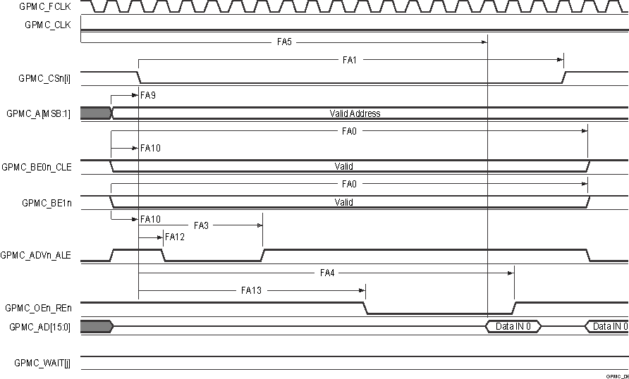
A. In GPMC_CSn[i], i is equal to 0,
1, 2 or 3. In GPMC_WAIT[j], jis equal to 0 or 1.
B. FA5 parameter illustrates amount
of time required to internally sample input data. It is expressed in number of
GPMC functional clock cycles. From start of read cycle and after FA5 functional
clock cycles, input data will be internally sampled by active functional clock
edge. FA5 value must be stored inside AccessTime register bits field.
C. GPMC_FCLK is an internal clock
(GPMC functional clock) not provided externally.
Figure 6-51 GPMC and
NOR Flash — Asynchronous Read — Single Word 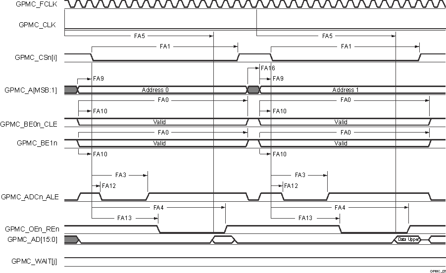
A. In GPMC_CSn[i], i is equal to 0,
1, 2 or 3. In GPMC_WAIT[j], j is equal to 0 or 1.
B. FA5 parameter illustrates amount
of time required to internally sample input data. It is expressed in number of
GPMC functional clock cycles. From start of read cycle and after FA5 functional
clock cycles, input data will be internally sampled by active functional clock
edge. FA5 value must be stored inside AccessTime register bits field.
C. GPMC_FCLK is an internal clock
(GPMC functional clock) not provided externally.
Figure 6-52 GPMC and
NOR Flash — Asynchronous Read — 32–Bit 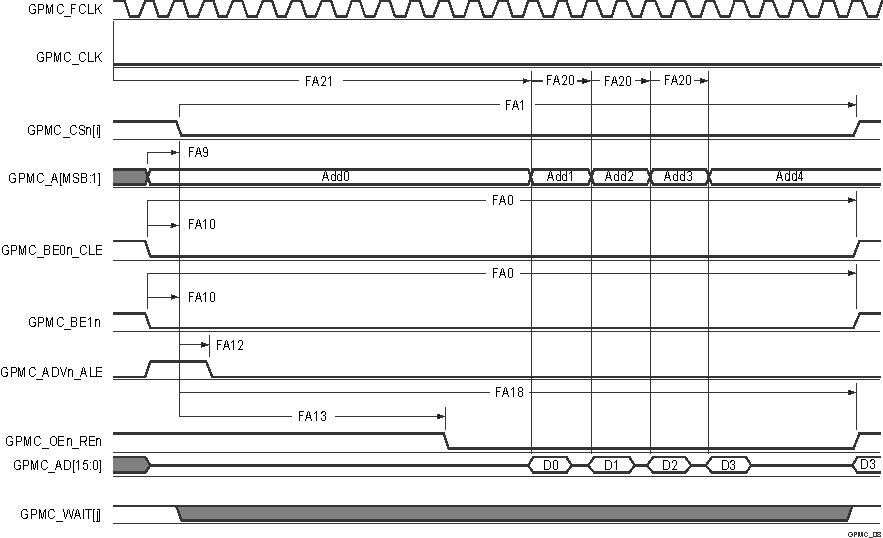
A. In GPMC_CSn[i], i is equal to 0,
1, 2 or 3. In GPMC_WAIT[j], j is equal to 0 or 1.
B. FA21 parameter illustrates
amount of time required to internally sample first input page data. It is
expressed in number of GPMC functional clock cycles. From start of read cycle
and after FA21 functional clock cycles, first input page data will be internally
sampled by active functional clock edge. FA21 calculation must be stored inside
AccessTime register bits field.
C. FA20 parameter illustrates
amount of time required to internally sample successive input page data. It is
expressed in number of GPMC functional clock cycles. After each access to input
page data, next input page data will be internally sampled by active functional
clock edge after FA20 functional clock cycles. FA20 is also the duration of
address phases for successive input page data (excluding first input page data).
FA20 value must be stored in PageBurstAccessTime register bits field.
D. GPMC_FCLK is an internal clock
(GPMC functional clock) not provided externally.
Figure 6-53 GPMC and
NOR Flash — Asynchronous Read — Page Mode 4x16–Bit 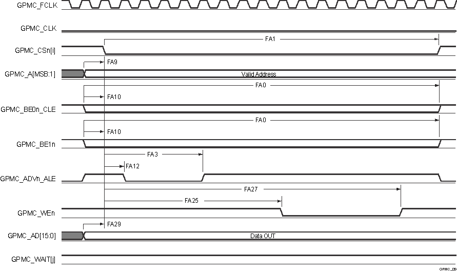
A. In GPMC_CSn[i], i is equal to 0,
1, 2 or 3. In GPMC_WAIT[j], j is equal to 0 or 1.
Figure 6-54 GPMC and
NOR Flash — Asynchronous Write — Single Word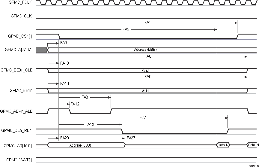
A. In GPMC_CSn[i], i is equal to 0,
1, 2 or 3. In GPMC_WAIT[j], j is equal to 0 or 1.
B. FA5 parameter illustrates amount
of time required to internally sample input data. It is expressed in number of
GPMC functional clock cycles. From start of read cycle and after FA5 functional
clock cycles, input data will be internally sampled by active functional clock
edge. FA5 value must be stored inside AccessTime register bits field.
C. GPMC_FCLK is an internal clock
(GPMC functional clock) not provided externally.
Figure 6-55 GPMC and
Multiplexed NOR Flash — Asynchronous Read — Single Word 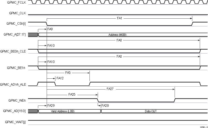
A. In GPMC_CSn[i], i is equal to 0,
1, 2 or 3. In GPMC_WAIT[j], j is equal to 0 or 1.
Figure 6-56 GPMC and
Multiplexed NOR Flash — Asynchronous Write — Single Word