JAJSL34G January   2021  – April 2024 AM6411 , AM6412 , AM6421 , AM6422 , AM6441 , AM6442

PRODUCTION DATA  

  1.   1
  2. 特長
  3. アプリケーション
  4. 概要
    1. 3.1 機能ブロック図
  5. Device Comparison
    1. 4.1 Related Products
  6. Terminal Configuration and Functions
    1. 5.1 Pin Diagrams
    2. 5.2 Pin Attributes
      1.      11
      2.      12
    3. 5.3 Signal Descriptions
      1.      14
      2. 5.3.1  ADC
        1. 5.3.1.1 MAIN Domain
          1.        17
      3. 5.3.2  CPSW3G
        1. 5.3.2.1 MAIN Domain
          1.        20
          2.        21
          3.        22
      4. 5.3.3  CPTS
        1. 5.3.3.1 MAIN Domain
          1.        25
          2.        26
      5. 5.3.4  DDRSS
        1. 5.3.4.1 MAIN Domain
          1.        29
      6. 5.3.5  ECAP
        1. 5.3.5.1 MAIN Domain
          1.        32
          2.        33
          3.        34
      7. 5.3.6  Emulation and Debug
        1. 5.3.6.1 MAIN Domain
          1.        37
        2. 5.3.6.2 MCU Domain
          1.        39
      8. 5.3.7  EPWM
        1. 5.3.7.1 MAIN Domain
          1.        42
          2.        43
          3.        44
          4.        45
          5.        46
          6.        47
          7.        48
          8.        49
          9.        50
          10.        51
      9. 5.3.8  EQEP
        1. 5.3.8.1 MAIN Domain
          1.        54
          2.        55
          3.        56
      10. 5.3.9  FSI
        1. 5.3.9.1 MAIN Domain
          1.        59
          2.        60
          3.        61
          4.        62
          5.        63
          6.        64
          7.        65
          8.        66
      11. 5.3.10 GPIO
        1. 5.3.10.1 MAIN Domain
          1.        69
          2.        70
        2. 5.3.10.2 MCU Domain
          1.        72
      12. 5.3.11 GPMC
        1. 5.3.11.1 MAIN Domain
          1.        75
      13. 5.3.12 I2C
        1. 5.3.12.1 MAIN Domain
          1.        78
          2.        79
          3.        80
          4.        81
        2. 5.3.12.2 MCU Domain
          1.        83
          2.        84
      14. 5.3.13 MCAN
        1. 5.3.13.1 MAIN Domain
          1.        87
          2.        88
      15. 5.3.14 MCSPI
        1. 5.3.14.1 MAIN Domain
          1.        91
          2.        92
          3.        93
          4.        94
          5.        95
        2. 5.3.14.2 MCU Domain
          1.        97
          2.        98
      16. 5.3.15 MDIO
        1. 5.3.15.1 MAIN Domain
          1.        101
      17. 5.3.16 MMC
        1. 5.3.16.1 MAIN Domain
          1.        104
          2.        105
      18. 5.3.17 OSPI
        1. 5.3.17.1 MAIN Domain
          1.        108
      19. 5.3.18 Power Supply
        1.       110
      20. 5.3.19 PRU_ICSSG
        1. 5.3.19.1 MAIN Domain
          1.        113
          2.        114
      21. 5.3.20 Reserved
        1.       116
      22. 5.3.21 SERDES
        1. 5.3.21.1 MAIN Domain
          1.        119
      23. 5.3.22 System and Miscellaneous
        1. 5.3.22.1 Boot Mode Configuration
          1. 5.3.22.1.1 MAIN Domain
            1.         123
        2. 5.3.22.2 Clock
          1. 5.3.22.2.1 MCU Domain
            1.         126
        3. 5.3.22.3 System
          1. 5.3.22.3.1 MAIN Domain
            1.         129
          2. 5.3.22.3.2 MCU Domain
            1.         131
        4. 5.3.22.4 VMON
          1.        133
      24. 5.3.23 TIMER
        1. 5.3.23.1 MAIN Domain
          1.        136
        2. 5.3.23.2 MCU Domain
          1.        138
      25. 5.3.24 UART
        1. 5.3.24.1 MAIN Domain
          1.        141
          2.        142
          3.        143
          4.        144
          5.        145
          6.        146
          7.        147
        2. 5.3.24.2 MCU Domain
          1.        149
          2.        150
      26. 5.3.25 USB
        1. 5.3.25.1 MAIN Domain
          1.        153
    4. 5.4 Pin Connectivity Requirements
  7. Specifications
    1. 6.1  Absolute Maximum Ratings
    2. 6.2  ESD Ratings
    3. 6.3  Power-On Hours (POH)
    4. 6.4  Recommended Operating Conditions
    5. 6.5  Operating Performance Points
    6. 6.6  Power Consumption Summary
    7. 6.7  Electrical Characteristics
      1. 6.7.1  I2C Open-Drain, and Fail-Safe (I2C OD FS) Electrical Characteristics
      2. 6.7.2  Fail-Safe Reset (FS RESET) Electrical Characteristics
      3. 6.7.3  High-Frequency Oscillator (HFOSC) Electrical Characteristics
      4. 6.7.4  eMMCPHY Electrical Characteristics
      5. 6.7.5  SDIO Electrical Characteristics
      6. 6.7.6  LVCMOS Electrical Characteristics
      7. 6.7.7  ADC12B Electrical Characteristics
      8. 6.7.8  USB2PHY Electrical Characteristics
      9. 6.7.9  SerDes PHY Electrical Characteristics
      10. 6.7.10 DDR Electrical Characteristics
    8. 6.8  VPP Specifications for One-Time Programmable (OTP) eFuses
      1. 6.8.1 Recommended Operating Conditions for OTP eFuse Programming
      2. 6.8.2 Hardware Requirements
      3. 6.8.3 Programming Sequence
      4. 6.8.4 Impact to Your Hardware Warranty
    9. 6.9  Thermal Resistance Characteristics
      1. 6.9.1 Thermal Resistance Characteristics
    10. 6.10 Timing and Switching Characteristics
      1. 6.10.1 Timing Parameters and Information
      2. 6.10.2 Power Supply Requirements
        1. 6.10.2.1 Power Supply Slew Rate Requirement
        2. 6.10.2.2 Power Supply Sequencing
          1. 6.10.2.2.1 Power-Up Sequencing
          2. 6.10.2.2.2 Power-Down Sequencing
      3. 6.10.3 System Timing
        1. 6.10.3.1 Reset Timing
        2. 6.10.3.2 Safety Signal Timing
        3. 6.10.3.3 Clock Timing
      4. 6.10.4 Clock Specifications
        1. 6.10.4.1 Input Clocks / Oscillators
          1. 6.10.4.1.1 MCU_OSC0 Internal Oscillator Clock Source
            1. 6.10.4.1.1.1 Load Capacitance
            2. 6.10.4.1.1.2 Shunt Capacitance
          2. 6.10.4.1.2 MCU_OSC0 LVCMOS Digital Clock Source
        2. 6.10.4.2 Output Clocks
        3. 6.10.4.3 PLLs
        4. 6.10.4.4 Recommended System Precautions for Clock and Control Signal Transitions
      5. 6.10.5 Peripherals
        1. 6.10.5.1  CPSW3G
          1. 6.10.5.1.1 CPSW3G MDIO Timing
          2. 6.10.5.1.2 CPSW3G RMII Timing
          3. 6.10.5.1.3 CPSW3G RGMII Timing
          4. 6.10.5.1.4 CPSW3G IOSETs
        2. 6.10.5.2  DDRSS
        3. 6.10.5.3  ECAP
        4. 6.10.5.4  EPWM
        5. 6.10.5.5  EQEP
        6. 6.10.5.6  FSI
        7. 6.10.5.7  GPIO
        8. 6.10.5.8  GPMC
          1. 6.10.5.8.1 GPMC and NOR Flash — Synchronous Mode
          2. 6.10.5.8.2 GPMC and NOR Flash — Asynchronous Mode
          3. 6.10.5.8.3 GPMC and NAND Flash — Asynchronous Mode
          4. 6.10.5.8.4 GPMC0 IOSETs
        9. 6.10.5.9  I2C
        10. 6.10.5.10 MCAN
        11. 6.10.5.11 MCSPI
          1. 6.10.5.11.1 MCSPI — Controller Mode
          2. 6.10.5.11.2 MCSPI — Peripheral Mode
        12. 6.10.5.12 MMCSD
          1. 6.10.5.12.1 MMC0 - eMMC Interface
            1. 6.10.5.12.1.1 Legacy SDR Mode
            2. 6.10.5.12.1.2 High Speed SDR Mode
            3. 6.10.5.12.1.3 High Speed DDR Mode
            4. 6.10.5.12.1.4 HS200 Mode
          2. 6.10.5.12.2 MMC1 - SD/SDIO Interface
            1. 6.10.5.12.2.1 Default Speed Mode
            2. 6.10.5.12.2.2 High Speed Mode
            3. 6.10.5.12.2.3 UHS–I SDR12 Mode
            4. 6.10.5.12.2.4 UHS–I SDR25 Mode
            5. 6.10.5.12.2.5 UHS–I SDR50 Mode
            6. 6.10.5.12.2.6 UHS–I DDR50 Mode
            7. 6.10.5.12.2.7 UHS–I SDR104 Mode
        13. 6.10.5.13 CPTS
        14. 6.10.5.14 OSPI
          1. 6.10.5.14.1 OSPI0 PHY Mode
            1. 6.10.5.14.1.1 OSPI0 With PHY Data Training
            2. 6.10.5.14.1.2 OSPI0 Without Data Training
              1. 6.10.5.14.1.2.1 OSPI0 PHY SDR Timing
              2. 6.10.5.14.1.2.2 OSPI0 PHY DDR Timing
          2. 6.10.5.14.2 OSPI0 Tap Mode
            1. 6.10.5.14.2.1 OSPI0 Tap SDR Timing
            2. 6.10.5.14.2.2 OSPI0 Tap DDR Timing
        15. 6.10.5.15 PCIe
        16. 6.10.5.16 PRU_ICSSG
          1. 6.10.5.16.1 PRU_ICSSG Programmable Real-Time Unit (PRU)
            1. 6.10.5.16.1.1 PRU_ICSSG PRU Direct Output Mode Timing
            2. 6.10.5.16.1.2 PRU_ICSSG PRU Parallel Capture Mode Timing
            3. 6.10.5.16.1.3 PRU_ICSSG PRU Shift Mode Timing
            4. 6.10.5.16.1.4 PRU_ICSSG PRU Sigma Delta and Peripheral Interface
              1. 6.10.5.16.1.4.1 PRU_ICSSG PRU Sigma Delta and Peripheral Interface Timing
          2. 6.10.5.16.2 PRU_ICSSG Pulse Width Modulation (PWM)
            1. 6.10.5.16.2.1 PRU_ICSSG PWM Timing
          3. 6.10.5.16.3 PRU_ICSSG Industrial Ethernet Peripheral (IEP)
            1. 6.10.5.16.3.1 PRU_ICSSG IEP Timing
          4. 6.10.5.16.4 PRU_ICSSG Universal Asynchronous Receiver Transmitter (UART)
            1. 6.10.5.16.4.1 PRU_ICSSG UART Timing
          5. 6.10.5.16.5 PRU_ICSSG Enhanced Capture Peripheral (ECAP)
            1. 6.10.5.16.5.1 PRU_ICSSG ECAP Timing
          6. 6.10.5.16.6 PRU_ICSSG RGMII, MII_RT, and Switch
            1. 6.10.5.16.6.1 PRU_ICSSG MDIO Timing
            2. 6.10.5.16.6.2 PRU_ICSSG MII Timing
            3. 6.10.5.16.6.3 PRU_ICSSG RGMII Timing
        17. 6.10.5.17 Timers
        18. 6.10.5.18 UART
        19. 6.10.5.19 USB
      6. 6.10.6 Emulation and Debug
        1. 6.10.6.1 Trace
        2. 6.10.6.2 JTAG
  8. Detailed Description
    1. 7.1 Overview
    2. 7.2 Processor Subsystems
      1. 7.2.1 Arm Cortex-A53 Subsystem
      2. 7.2.2 Arm Cortex-R5F Subsystem (R5FSS)
      3. 7.2.3 Arm Cortex-M4F (M4FSS)
    3. 7.3 Accelerators and Coprocessors
      1. 7.3.1 Programmable Real-Time Unit Subsystem and Industrial Communication Subsystem (PRU_ICSSG)
    4. 7.4 Other Subsystems
      1. 7.4.1 PDMA Controller
      2. 7.4.2 Peripherals
        1. 7.4.2.1  ADC
        2. 7.4.2.2  DCC
        3. 7.4.2.3  Dual Date Rate (DDR) External Memory Interface (DDRSS)
        4. 7.4.2.4  ECAP
        5. 7.4.2.5  EPWM
        6. 7.4.2.6  ELM
        7. 7.4.2.7  ESM
        8. 7.4.2.8  GPIO
        9. 7.4.2.9  EQEP
        10. 7.4.2.10 General-Purpose Memory Controller (GPMC)
        11. 7.4.2.11 I2C
        12. 7.4.2.12 MCAN
        13. 7.4.2.13 MCRC Controller
        14. 7.4.2.14 MCSPI
        15. 7.4.2.15 MMCSD
        16. 7.4.2.16 OSPI
        17. 7.4.2.17 Peripheral Component Interconnect Express (PCIe)
        18. 7.4.2.18 Serializer/Deserializer (SerDes) PHY
        19. 7.4.2.19 Real Time Interrupt (RTI/WWDT)
        20. 7.4.2.20 Dual Mode Timer (DMTIMER)
        21. 7.4.2.21 UART
        22. 7.4.2.22 Universal Serial Bus Subsystem (USBSS)
  9. Applications, Implementation, and Layout
    1. 8.1 Device Connection and Layout Fundamentals
      1. 8.1.1 Power Supply
        1. 8.1.1.1 Power Supply Designs
        2. 8.1.1.2 Power Distribution Network Implementation Guidance
      2. 8.1.2 External Oscillator
      3. 8.1.3 JTAG, EMU, and TRACE
      4. 8.1.4 Unused Pins
    2. 8.2 Peripheral- and Interface-Specific Design Information
      1. 8.2.1 DDR Board Design and Layout Guidelines
      2. 8.2.2 OSPI/QSPI/SPI Board Design and Layout Guidelines
        1. 8.2.2.1 No Loopback, Internal PHY Loopback, and Internal Pad Loopback
        2. 8.2.2.2 External Board Loopback
        3. 8.2.2.3 DQS (only available in Octal SPI devices)
      3. 8.2.3 USB VBUS Design Guidelines
      4. 8.2.4 System Power Supply Monitor Design Guidelines
      5. 8.2.5 High Speed Differential Signal Routing Guidance
      6. 8.2.6 Thermal Solution Guidance
    3. 8.3 Clock Routing Guidelines
      1. 8.3.1 Oscillator Routing
  10. Device and Documentation Support
    1. 9.1 Device Nomenclature
      1. 9.1.1 Standard Package Symbolization
      2. 9.1.2 Device Naming Convention
    2. 9.2 Tools and Software
    3. 9.3 Documentation Support
    4. 9.4 サポート・リソース
    5. 9.5 Trademarks
    6. 9.6 静電気放電に関する注意事項
    7. 9.7 用語集
  11. 10Revision History
  12. 11Mechanical, Packaging, and Orderable Information
    1. 11.1 Packaging Information

パッケージ・オプション

デバイスごとのパッケージ図は、PDF版データシートをご参照ください。

メカニカル・データ(パッケージ|ピン)
  • ALV|441
サーマルパッド・メカニカル・データ
発注情報
Power-Down Sequencing

Figure 6-6 describes the device power-down sequencing.
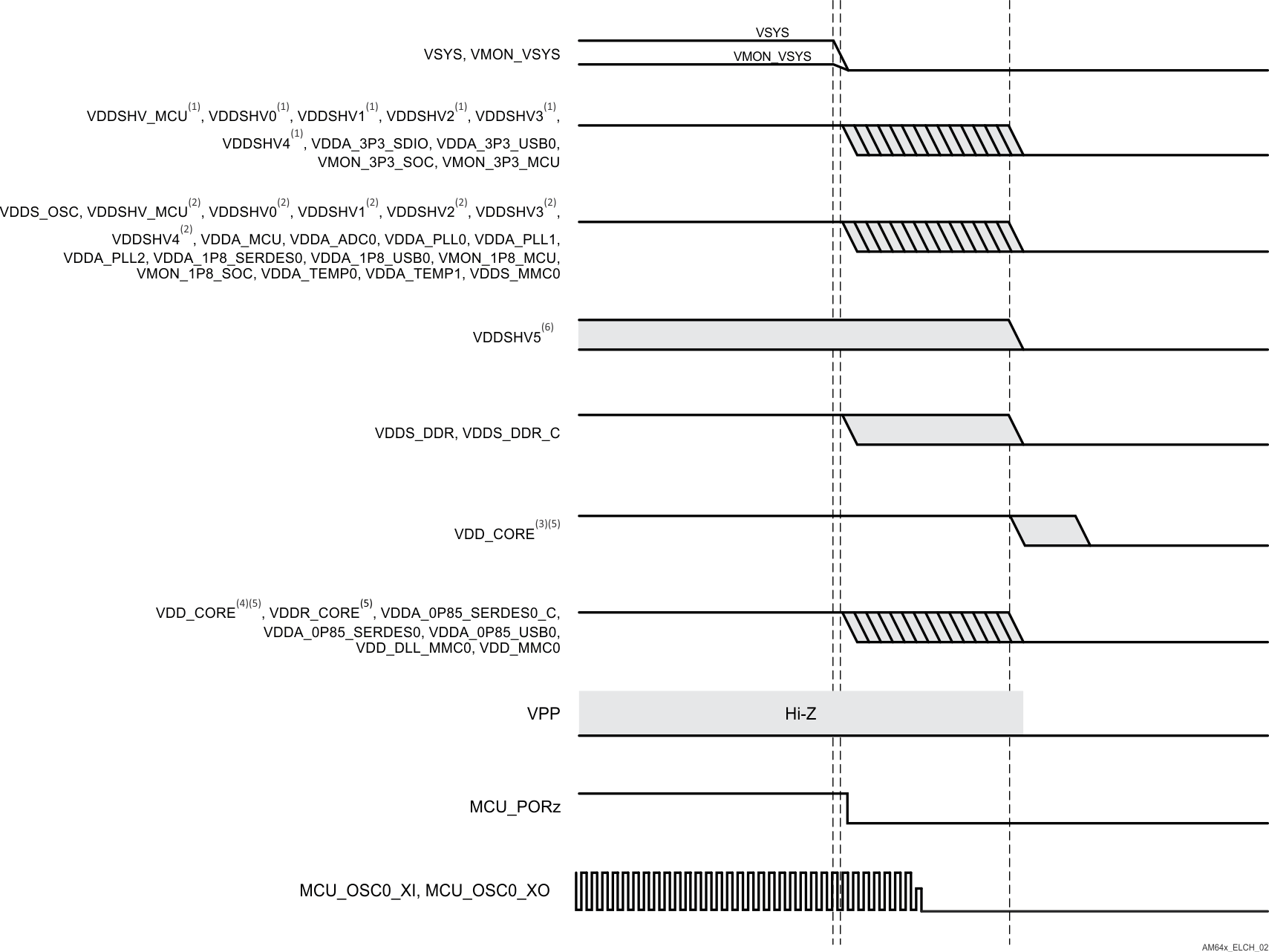
AM6442 AM6441 AM6422 AM6421 AM6412 AM6411 Power-Down Sequencing Figure 6-6 Power-Down Sequencing
  1. VDDSHV_MCU and VDDSHVx [x=0-5] when operating at 3.3V.
  2. VDDSHV_MCU and VDDSHVx [x=0-5] when operating at 1.8V.
  3. VDD_CORE when operating at 0.75V.
  4. VDD_CORE when operating at 0.85V.
  5. The potential applied to VDDR_CORE must never be greater than the potential applied to VDD_CORE + 0.18V during power-up or power-down. This requires VDD_CORE to ramp up before and ramp down after VDDR_CORE when VDD_CORE is operating at 0.75V. VDD_CORE does not have any ramp requirements beyond the one defined for VDDR_CORE. VDD_CORE and VDDR_CORE are expected to be powered by the same source so they ramp together when VDD_CORE is operating at 0.85V.
  6. VDDSHV5 was designed to support power-up, power-down, or dynamic voltage change without any dependency on other power rails. This capability is required to support UHS-I SD Cards.