JAJSL34G January 2021 – April 2024 AM6411 , AM6412 , AM6421 , AM6422 , AM6441 , AM6442
PRODUCTION DATA
- 1
- 1 特長
- 2 アプリケーション
- 3 概要
- 4 Device Comparison
-
5 Terminal Configuration and Functions
- 5.1 Pin Diagrams
- 5.2 Pin Attributes
- 5.3
Signal Descriptions
- 14
- 5.3.1 ADC
- 5.3.2 CPSW3G
- 5.3.3 CPTS
- 5.3.4 DDRSS
- 5.3.5 ECAP
- 5.3.6 Emulation and Debug
- 5.3.7 EPWM
- 5.3.8 EQEP
- 5.3.9 FSI
- 5.3.10 GPIO
- 5.3.11 GPMC
- 5.3.12 I2C
- 5.3.13 MCAN
- 5.3.14 MCSPI
- 5.3.15 MDIO
- 5.3.16 MMC
- 5.3.17 OSPI
- 5.3.18 Power Supply
- 5.3.19 PRU_ICSSG
- 5.3.20 Reserved
- 5.3.21 SERDES
- 5.3.22 System and Miscellaneous
- 5.3.23 TIMER
- 5.3.24 UART
- 5.3.25 USB
- 5.4 Pin Connectivity Requirements
-
6 Specifications
- 6.1 Absolute Maximum Ratings
- 6.2 ESD Ratings
- 6.3 Power-On Hours (POH)
- 6.4 Recommended Operating Conditions
- 6.5 Operating Performance Points
- 6.6 Power Consumption Summary
- 6.7
Electrical
Characteristics
- 6.7.1 I2C Open-Drain, and Fail-Safe (I2C OD FS) Electrical Characteristics
- 6.7.2 Fail-Safe Reset (FS RESET) Electrical Characteristics
- 6.7.3 High-Frequency Oscillator (HFOSC) Electrical Characteristics
- 6.7.4 eMMCPHY Electrical Characteristics
- 6.7.5 SDIO Electrical Characteristics
- 6.7.6 LVCMOS Electrical Characteristics
- 6.7.7 ADC12B Electrical Characteristics
- 6.7.8 USB2PHY Electrical Characteristics
- 6.7.9 SerDes PHY Electrical Characteristics
- 6.7.10 DDR Electrical Characteristics
- 6.8 VPP Specifications for One-Time Programmable (OTP) eFuses
- 6.9 Thermal Resistance Characteristics
- 6.10
Timing and Switching Characteristics
- 6.10.1 Timing Parameters and Information
- 6.10.2 Power Supply Requirements
- 6.10.3 System Timing
- 6.10.4 Clock Specifications
- 6.10.5
Peripherals
- 6.10.5.1 CPSW3G
- 6.10.5.2 DDRSS
- 6.10.5.3 ECAP
- 6.10.5.4 EPWM
- 6.10.5.5 EQEP
- 6.10.5.6 FSI
- 6.10.5.7 GPIO
- 6.10.5.8 GPMC
- 6.10.5.9 I2C
- 6.10.5.10 MCAN
- 6.10.5.11 MCSPI
- 6.10.5.12 MMCSD
- 6.10.5.13 CPTS
- 6.10.5.14 OSPI
- 6.10.5.15 PCIe
- 6.10.5.16
PRU_ICSSG
- 6.10.5.16.1 PRU_ICSSG Programmable Real-Time Unit (PRU)
- 6.10.5.16.2 PRU_ICSSG Pulse Width Modulation (PWM)
- 6.10.5.16.3 PRU_ICSSG Industrial Ethernet Peripheral (IEP)
- 6.10.5.16.4 PRU_ICSSG Universal Asynchronous Receiver Transmitter (UART)
- 6.10.5.16.5 PRU_ICSSG Enhanced Capture Peripheral (ECAP)
- 6.10.5.16.6 PRU_ICSSG RGMII, MII_RT, and Switch
- 6.10.5.17 Timers
- 6.10.5.18 UART
- 6.10.5.19 USB
- 6.10.6 Emulation and Debug
-
7 Detailed Description
- 7.1 Overview
- 7.2 Processor Subsystems
- 7.3 Accelerators and Coprocessors
- 7.4
Other Subsystems
- 7.4.1 PDMA Controller
- 7.4.2
Peripherals
- 7.4.2.1 ADC
- 7.4.2.2 DCC
- 7.4.2.3 Dual Date Rate (DDR) External Memory Interface (DDRSS)
- 7.4.2.4 ECAP
- 7.4.2.5 EPWM
- 7.4.2.6 ELM
- 7.4.2.7 ESM
- 7.4.2.8 GPIO
- 7.4.2.9 EQEP
- 7.4.2.10 General-Purpose Memory Controller (GPMC)
- 7.4.2.11 I2C
- 7.4.2.12 MCAN
- 7.4.2.13 MCRC Controller
- 7.4.2.14 MCSPI
- 7.4.2.15 MMCSD
- 7.4.2.16 OSPI
- 7.4.2.17 Peripheral Component Interconnect Express (PCIe)
- 7.4.2.18 Serializer/Deserializer (SerDes) PHY
- 7.4.2.19 Real Time Interrupt (RTI/WWDT)
- 7.4.2.20 Dual Mode Timer (DMTIMER)
- 7.4.2.21 UART
- 7.4.2.22 Universal Serial Bus Subsystem (USBSS)
-
8 Applications,
Implementation, and Layout
- 8.1 Device Connection and Layout Fundamentals
- 8.2 Peripheral- and Interface-Specific Design Information
- 8.3 Clock Routing Guidelines
- 9 Device and Documentation Support
- 10Revision History
- 11Mechanical, Packaging, and Orderable Information
パッケージ・オプション
デバイスごとのパッケージ図は、PDF版データシートをご参照ください。
メカニカル・データ(パッケージ|ピン)
- ALV|441
サーマルパッド・メカニカル・データ
発注情報
6.10.5.8.1 GPMC and NOR Flash — Synchronous Mode
Hold time, input wait GPMC_WAIT[j] valid after output clock GPMC_CLK high (th(clkH-waitV))
Hold time, input wait GPMC_WAIT[j] valid after output clock GPMC_CLK high (th(clkH-waitV))
Table 6-54 and Table 6-55 present timing requirements and switching characteristics for GPMC and NOR Flash - Synchronous Mode.
Table 6-54 GPMC and NOR Flash Timing Requirements — Synchronous Mode see Figure 6-39,
Figure 6-40, and
Figure 6-43
| NO. | PARAMETER | DESCRIPTION | MODE(5) | MIN | MAX | MIN | MAX | UNIT |
|---|---|---|---|---|---|---|---|---|
| GPMC_FCLK = 100 MHz(2) | GPMC_FCLK = 133 MHz(2) | |||||||
| F12 | tsu(dV-clkH) | Setup time, input data GPMC_AD[n:0](1) valid before output clock GPMC_CLK high | div_by_1_mode; GPMC_FCLK_MUX; TIMEPARAGRANULARITY_X1 |
1.81 | 1.12 | ns | ||
| not_div_by_1_mode; GPMC_FCLK_MUX; TIMEPARAGRANULARITY_X1 |
1.06 | 3.5 | ns | |||||
| F13 | th(clkH-dV) | Hold time, input data GPMC_AD[n:0](1) valid after output clock GPMC_CLK high | div_by_1_mode; GPMC_FCLK_MUX; TIMEPARAGRANULARITY_X1 |
2.29 | 2.29 | ns | ||
| not_div_by_1_mode; GPMC_FCLK_MUX; TIMEPARAGRANULARITY_X1 |
2.29 | 2.29 | ns | |||||
| F21 | tsu(waitV-clkH) | Setup time, input wait GPMC_WAIT[j](3)(4) valid before output clock GPMC_CLK high | div_by_1_mode; GPMC_FCLK_MUX; TIMEPARAGRANULARITY_X1 |
1.81 | 1.12 | ns | ||
| not_div_by_1_mode; GPMC_FCLK_MUX; TIMEPARAGRANULARITY_X1 |
1.06 | 3.5 | ns | |||||
| F22 | th(clkH-waitV) | Hold time, input wait GPMC_WAIT[j](3)(4) valid after output clock GPMC_CLK high | div_by_1_mode; GPMC_FCLK_MUX; TIMEPARAGRANULARITY_X1 |
2.29 | 2.29 | ns | ||
| not_div_by_1_mode; GPMC_FCLK_MUX; TIMEPARAGRANULARITY_X1 |
2.29 | 2.29 | ns | |||||
(1) Synchronous Mode supports 16-bit data bus up to 133 MHz and 32-bit data bus up
to 100 MHz
(2) GPMC_FCLK select
- gpmc_fclk_sel[1:0] = 2b01 to select the 100MHz GPMC_FCLK
- gpmc_fclk_sel[1:0] = 2b00 to select the 133MHz GPMC_FCLK
(3) In
GPMC_WAIT[j], j is equal to 0 or 1.
(4) Wait
monitoring support is limited to a WaitMonitoringTime value > 0. For a full
description of wait monitoring feature, see General-Purpose Memory Controller
(GPMC) section in the device TRM.
(5) For
div_by_1_mode:
For not_div_by_1_mode:
For GPMC_FCLK_MUX:
For TIMEPARAGRANULARITY_X1:
- GPMC_CONFIG1_i Register:
GPMCFCLKDIVIDER = 0h:
- GPMC_CLK frequency = GPMC_FCLK frequency
For not_div_by_1_mode:
- GPMC_CONFIG1_i Register:
GPMCFCLKDIVIDER = 1h to 3h:
- GPMC_CLK frequency = GPMC_FCLK frequency / (2 to 4)
For GPMC_FCLK_MUX:
- CTRLMMR_GPMC_CLKSEL[1-0] CLK_SEL = 01 = PER1_PLL_CLKOUT / 3 = 300 / 3 = 100MHz
For TIMEPARAGRANULARITY_X1:
- GPMC_CONFIG1_i Register: TIMEPARAGRANULARITY = 0h = x1 latencies (affecting RD/WRCYCLETIME, RD/WRACCESSTIME, PAGEBURSTACCESSTIME, CSONTIME, CSRD/WROFFTIME, ADVONTIME, ADVRD/WROFFTIME, OEONTIME, OEOFFTIME, WEONTIME, WEOFFTIME, CYCLE2CYCLEDELAY, BUSTURNAROUND, TIMEOUTSTARTVALUE, WRDATAONADMUXBUS)
Table 6-55 GPMC and NOR Flash Switching Characteristics – Synchronous Mode see Figure 6-39,
Figure 6-40, Figure 6-41, Figure 6-42, and Figure 6-43
| NO.(3) | PARAMETER | DESCRIPTION | MODE(17) | MIN | MAX | MIN | MAX | UNIT |
|---|---|---|---|---|---|---|---|---|
| 100 MHz | 133 MHz | |||||||
| F0 | 1 / tc(clk) | Period, output clock GPMC_CLK(16) | div_by_1_mode; GPMC_FCLK_MUX; TIMEPARAGRANULARITY_X1 |
10.00 | 7.52 | ns | ||
| F1 | tw(clkH) | Typical pulse duration, output clock GPMC_CLK high | div_by_1_mode; GPMC_FCLK_MUX; TIMEPARAGRANULARITY_X1 |
0.475P - 0.3(15) | 0.475P - 0.3(15) | ns | ||
| F1 | tw(clkL) | Typical pulse duration, output clock GPMC_CLK low | div_by_1_mode; GPMC_FCLK_MUX; TIMEPARAGRANULARITY_X1 |
0.475P - 0.3(15) | 0.475P - 0.3(15) | ns | ||
| F2 | td(clkH-csnV) | Delay time, output clock GPMC_CLK rising edge to output chip select GPMC_CSn[i] transition(14) | div_by_1_mode; GPMC_FCLK_MUX; TIMEPARAGRANULARITY_X1; no extra_delay |
F - 2.2 (6) | F + 3.75 | F - 2.2 (6) | F + 3.75 | ns |
| F3 | td(clkH-CSn[i]V) | Delay time, output clock GPMC_CLK rising edge to output chip select GPMC_CSn[i] invalid(14) | div_by_1_mode; GPMC_FCLK_MUX; TIMEPARAGRANULARITY_X1; no extra_delay |
E - 2.2 (5) | E + 3.18 | E - 2.2 (5) | E + 4.5 | ns |
| F4 | td(aV-clk) | Delay time, output address GPMC_A[27:1] valid to output clock GPMC_CLK first edge | div_by_1_mode; GPMC_FCLK_MUX; TIMEPARAGRANULARITY_X1 |
B - 2.3 (3) | B + 4.5 | B - 2.3 (3) | B + 4.5 | ns |
| F5 | td(clkH-aIV) | Delay time, output clock GPMC_CLK rising edge to output address GPMC_A[27:1] invalid | div_by_1_mode; GPMC_FCLK_MUX; TIMEPARAGRANULARITY_X1 |
-2.3 | 4.5 | -2.3 | 4.5 | ns |
| F6 | td(be[x]nV-clk) | Delay time, output lower byte enable and command latch enable GPMC_BE0n_CLE, output upper byte enable GPMC_BE1n valid to output clock GPMC_CLK first edge | div_by_1_mode; GPMC_FCLK_MUX; TIMEPARAGRANULARITY_X1 |
B - 2.3 (3) | B + 1.9 | B - 2.3 (3) | B + 1.9 | ns |
| F7 | td(clkH-be[x]nIV) | Delay time, output clock GPMC_CLK rising edge to output lower byte enable and command latch enable GPMC_BE0n_CLE, output upper byte enable GPMC_BE1n invalid(11) | div_by_1_mode; GPMC_FCLK_MUX; TIMEPARAGRANULARITY_X1 |
D - 2.3(4) | D + 1.9 | D - 2.3 (4) | D + 1.9 | ns |
| F7 | td(clkL-be[x]nIV) | Delay time, GPMC_CLK falling edge to GPMC_BE0n_CLE, GPMC_BE1n invalid(12) | div_by_1_mode; GPMC_FCLK_MUX; TIMEPARAGRANULARITY_X1 |
D - 2.3 (4) | D + 1.9 | D - 2.3 (4) | D + 1.9 | ns |
| F7 | td(clkL-be[x]nIV). | Delay time, GPMC_CLK falling edge to GPMC_BE0n_CLE, GPMC_BE1n invalid(13) | div_by_1_mode; GPMC_FCLK_MUX; TIMEPARAGRANULARITY_X1 |
D - 2.3 (4) | D + 1.9 | D - 2.3 (4) | D + 1.9 | ns |
| F8 | td(clkH-advn) | Delay time, output clock GPMC_CLK rising edge to output address valid and address latch enable GPMC_ADVn_ALE transition | div_by_1_mode; GPMC_FCLK_MUX; TIMEPARAGRANULARITY_X1; no extra_delay |
G - 2.3(7) | G + 4.5 | G - 2.3 (7) | G + 4.5 | ns |
| F9 | td(clkH-advnIV) | Delay time, output clock GPMC_CLK rising edge to output address valid and address latch enable GPMC_ADVn_ALE invalid | div_by_1_mode; GPMC_FCLK_MUX; TIMEPARAGRANULARITY_X1; no extra_delay |
D - 2.3 (4) | D + 4.5 | D - 2.3 (4) | D + 4.5 | ns |
| F10 | td(clkH-oen) | Delay time, output clock GPMC_CLK rising edge to output enable GPMC_OEn_REn transition | div_by_1_mode; GPMC_FCLK_MUX; TIMEPARAGRANULARITY_X1; no extra_delay |
H - 2.3(8) | H + 3.5 | H - 2.3 (8) | H + 3.5 | ns |
| F11 | td(clkH-oenIV) | Delay time, output clock GPMC_CLK rising edge to output enable GPMC_OEn_REn invalid | div_by_1_mode; GPMC_FCLK_MUX; TIMEPARAGRANULARITY_X1; no extra_delay |
H - 2.3 (8) | H + 3.5 | H - 2.3 (8) | H + 3.5 | ns |
| F14 | td(clkH-wen) | Delay time, output clock GPMC_CLK rising edge to output write enable GPMC_WEn transition | div_by_1_mode; GPMC_FCLK_MUX; TIMEPARAGRANULARITY_X1; no extra_delay |
I - 2.3 (9) | I + 4.5 | I - 2.3 (9) | I + 4.5 | ns |
| F15 | td(clkH-do) | Delay time, output clock GPMC_CLK rising edge to output data GPMC_AD[n:0](1) transition(11) | div_by_1_mode; GPMC_FCLK_MUX; TIMEPARAGRANULARITY_X1 |
J - 2.3 (10) | J + 2.7 | J - 2.3 (10) | J + 2.7 | ns |
| F15 | td(clkL-do) | Delay time, GPMC_CLK falling edge to GPMC_AD[n:0](1) data bus transition(12) | div_by_1_mode; GPMC_FCLK_MUX; TIMEPARAGRANULARITY_X1 |
J - 2.3 (10) | J + 2.7 | J - 2.3 (10) | J + 2.7 | ns |
| F15 | td(clkL-do). | Delay time, GPMC_CLK falling edge to GPMC_AD[n:0](1) data bus transition(13) | div_by_1_mode; GPMC_FCLK_MUX; TIMEPARAGRANULARITY_X1 |
J - 2.3 (10) | J + 2.7 | J - 2.3 (10) | J + 2.7 | ns |
| F17 | td(clkH-be[x]n) | Delay time, output clock GPMC_CLK rising edge to output lower byte enable and command latch enable GPMC_BE0n_CLE transition(11) | div_by_1_mode; GPMC_FCLK_MUX; TIMEPARAGRANULARITY_X1 |
J - 2.3 (10) | J + 1.9 | J - 2.3 (10) | J + 1.9 | ns |
| F17 | td(clkL-be[x]n) | Delay time, GPMC_CLK falling edge to GPMC_BE0n_CLE, GPMC_BE1n transition(12) | div_by_1_mode; GPMC_FCLK_MUX; TIMEPARAGRANULARITY_X1 |
J - 2.3 (10) | J + 1.9 | J - 2.3 (10) | J + 1.9 | ns |
| F17 | td(clkL-be[x]n). | Delay time, GPMC_CLK falling edge to GPMC_BE0n_CLE, GPMC_BE1n transition(13) | div_by_1_mode; GPMC_FCLK_MUX; TIMEPARAGRANULARITY_X1 |
J - 2.3 (10) | J + 1.9 | J - 2.3 (10) | J + 1.9 | ns |
| F18 | tw(csnV) | Pulse duration, output chip select GPMC_CSn[i](14) low | Read | A | A | ns | ||
| Write | A | A | ns | |||||
| F19 | tw(be[x]nV) | Pulse duration, output lower byte enable and command latch enable GPMC_BE0n_CLE, output upper byte enable GPMC_BE1n low | Read | C | C | ns | ||
| Write | C | C | ns | |||||
| F20 | tw(advnV) | Pulse duration, output address valid and address latch enable GPMC_ADVn_ALE low | Read | K | K | ns | ||
| Write | K | K | ns | |||||
(1) Synchronous Mode supports 16-bit data bus up to 133 MHz and 32-bit data bus up
to 100 MHz
(3) B =
ClkActivationTime × GPMC_FCLK(15)
(4) For
single read: D = (RdCycleTime - AccessTime) × (TimeParaGranularity + 1) ×
GPMC_FCLK(15)
For burst read: D = (RdCycleTime - AccessTime) × (TimeParaGranularity + 1) × GPMC_FCLK(15)
For burst write: D = (WrCycleTime - AccessTime) × (TimeParaGranularity + 1) × GPMC_FCLK(15)
For burst read: D = (RdCycleTime - AccessTime) × (TimeParaGranularity + 1) × GPMC_FCLK(15)
For burst write: D = (WrCycleTime - AccessTime) × (TimeParaGranularity + 1) × GPMC_FCLK(15)
(5) For
single read: E = (CSRdOffTime - AccessTime) × (TimeParaGranularity + 1) ×
GPMC_FCLK(15)
For burst read: E = (CSRdOffTime - AccessTime) × (TimeParaGranularity + 1) × GPMC_FCLK(15)
For burst write: E = (CSWrOffTime - AccessTime) × (TimeParaGranularity + 1) × GPMC_FCLK(15)
For burst read: E = (CSRdOffTime - AccessTime) × (TimeParaGranularity + 1) × GPMC_FCLK(15)
For burst write: E = (CSWrOffTime - AccessTime) × (TimeParaGranularity + 1) × GPMC_FCLK(15)
(6) For
csn falling edge (CS activated):
- Case GPMCFCLKDIVIDER = 0:
- F = 0.5 × CSExtraDelay × GPMC_FCLK(15)
- Case GPMCFCLKDIVIDER = 1:
- Case GPMCFCLKDIVIDER = 2:
- F = 0.5 × CSExtraDelay × GPMC_FCLK(15) if ((CSOnTime - ClkActivationTime) is a multiple of 3)
- F = (1 + 0.5 × CSExtraDelay) × GPMC_FCLK(15) if ((CSOnTime - ClkActivationTime - 1) is a multiple of 3)
- F = (2 + 0.5 × CSExtraDelay) × GPMC_FCLK(15) if ((CSOnTime - ClkActivationTime - 2) is a multiple of 3)
(7) For
ADV falling edge (ADV activated):
For ADV rising edge (ADV deactivated) in Reading mode:
For ADV rising edge (ADV deactivated) in Writing mode:
- Case GPMCFCLKDIVIDER = 0:
- G = 0.5 × ADVExtraDelay × GPMC_FCLK(15)
- Case GPMCFCLKDIVIDER = 1:
- Case GPMCFCLKDIVIDER = 2:
- G = 0.5 × ADVExtraDelay × GPMC_FCLK(15) if ((ADVOnTime - ClkActivationTime) is a multiple of 3)
- G = (1 + 0.5 × ADVExtraDelay) × GPMC_FCLK(15) if ((ADVOnTime - ClkActivationTime - 1) is a multiple of 3)
- G = (2 + 0.5 × ADVExtraDelay) × GPMC_FCLK(15) if ((ADVOnTime - ClkActivationTime - 2) is a multiple of 3)
For ADV rising edge (ADV deactivated) in Reading mode:
- Case GPMCFCLKDIVIDER = 0:
- G = 0.5 × ADVExtraDelay × GPMC_FCLK(15)
- Case GPMCFCLKDIVIDER = 1:
- Case GPMCFCLKDIVIDER = 2:
- G = 0.5 × ADVExtraDelay × GPMC_FCLK(15) if ((ADVRdOffTime - ClkActivationTime) is a multiple of 3)
- G = (1 + 0.5 × ADVExtraDelay) × GPMC_FCLK(15) if ((ADVRdOffTime - ClkActivationTime - 1) is a multiple of 3)
- G = (2 + 0.5 × ADVExtraDelay) × GPMC_FCLK(15) if ((ADVRdOffTime - ClkActivationTime - 2) is a multiple of 3)
For ADV rising edge (ADV deactivated) in Writing mode:
- Case GPMCFCLKDIVIDER = 0:
- G = 0.5 × ADVExtraDelay × GPMC_FCLK(15)
- Case GPMCFCLKDIVIDER = 1:
- Case GPMCFCLKDIVIDER = 2:
- G = 0.5 × ADVExtraDelay × GPMC_FCLK(15) if ((ADVWrOffTime - ClkActivationTime) is a multiple of 3)
- G = (1 + 0.5 × ADVExtraDelay) × GPMC_FCLK(15) if ((ADVWrOffTime - ClkActivationTime - 1) is a multiple of 3)
- G = (2 + 0.5 × ADVExtraDelay) × GPMC_FCLK(15) if ((ADVWrOffTime - ClkActivationTime - 2) is a multiple of 3)
(8) For
OE falling edge (OE activated) and IO DIR rising edge (Data Bus input
direction):
For OE rising edge (OE deactivated):
- Case GPMCFCLKDIVIDER = 0:
- H = 0.5 × OEExtraDelay × GPMC_FCLK(15)
- Case GPMCFCLKDIVIDER = 1:
- Case GPMCFCLKDIVIDER = 2:
- H = 0.5 × OEExtraDelay × GPMC_FCLK(15) if ((OEOnTime - ClkActivationTime) is a multiple of 3)
- H = (1 + 0.5 × OEExtraDelay) × GPMC_FCLK(15) if ((OEOnTime - ClkActivationTime - 1) is a multiple of 3)
- H = (2 + 0.5 × OEExtraDelay) × GPMC_FCLK(15) if ((OEOnTime - ClkActivationTime - 2) is a multiple of 3)
For OE rising edge (OE deactivated):
- Case GPMCFCLKDIVIDER = 0:
- H = 0.5 × OEExtraDelay × GPMC_FCLK(15)
- Case GPMCFCLKDIVIDER = 1:
- Case GPMCFCLKDIVIDER = 2:
- H = 0.5 × OEExtraDelay × GPMC_FCLK(15) if ((OEOffTime - ClkActivationTime) is a multiple of 3)
- H = (1 + 0.5 × OEExtraDelay) × GPMC_FCLK(15) if ((OEOffTime - ClkActivationTime - 1) is a multiple of 3)
- H = (2 + 0.5 × OEExtraDelay) × GPMC_FCLK(15) if ((OEOffTime - ClkActivationTime - 2) is a multiple of 3)
(9) For
WE falling edge (WE activated):
For WE rising edge (WE deactivated):
- Case GPMCFCLKDIVIDER = 0:
- I = 0.5 × WEExtraDelay × GPMC_FCLK(15)
- Case GPMCFCLKDIVIDER = 1:
- Case GPMCFCLKDIVIDER = 2:
- I = 0.5 × WEExtraDelay × GPMC_FCLK(15) if ((WEOnTime - ClkActivationTime) is a multiple of 3)
- I = (1 + 0.5 × WEExtraDelay) × GPMC_FCLK(15) if ((WEOnTime - ClkActivationTime - 1) is a multiple of 3)
- I = (2 + 0.5 × WEExtraDelay) × GPMC_FCLK(15) if ((WEOnTime - ClkActivationTime - 2) is a multiple of 3)
For WE rising edge (WE deactivated):
- Case GPMCFCLKDIVIDER = 0:
- I = 0.5 × WEExtraDelay × GPMC_FCLK (15)
- Case GPMCFCLKDIVIDER = 1:
- Case GPMCFCLKDIVIDER = 2:
- I = 0.5 × WEExtraDelay × GPMC_FCLK(15) if ((WEOffTime - ClkActivationTime) is a multiple of 3)
- I = (1 + 0.5 × WEExtraDelay) × GPMC_FCLK(15) if ((WEOffTime - ClkActivationTime - 1) is a multiple of 3)
- I = (2 + 0.5 × WEExtraDelay) × GPMC_FCLK(15) if ((WEOffTime - ClkActivationTime - 2) is a multiple of 3)
(10) J
= GPMC_FCLK(15)
(11) First transfer only for CLK DIV 1 mode.
(12) Half cycle; for all data after initial transfer for CLK DIV 1 mode.
(13) Half cycle of GPMC_CLKOUT; for all data for modes other than CLK DIV 1 mode.
GPMC_CLKOUT divide down from GPMC_FCLK.
(14) In
GPMC_CSn[i], i is equal to 0, 1, 2 or 3. In GPMC_WAIT[j], j is equal to 0 or
1.
(15) P
= GPMC_CLK period in ns
(16) Related to the GPMC_CLK output clock maximum and minimum frequencies
programmable in the GPMC module by setting the GPMC_CONFIG1_i configuration
register bit field GPMCFCLKDIVIDER.
(17) For div_by_1_mode:
For GPMC_FCLK_MUX:
For TIMEPARAGRANULARITY_X1:
For no extra_delay:
- GPMC_CONFIG1_i register:
GPMCFCLKDIVIDER = 0h:
- GPMC_CLK frequency = GPMC_FCLK frequency
For GPMC_FCLK_MUX:
- CTRLMMR_GPMC_CLKSEL[1-0] CLK_SEL = 01 = PER1_PLL_CLKOUT / 3 = 300 / 3 = 100MHz
For TIMEPARAGRANULARITY_X1:
- GPMC_CONFIG1_i Register: TIMEPARAGRANULARITY = 0h = x1 latencies (affecting RD/WRCYCLETIME, RD/WRACCESSTIME, PAGEBURSTACCESSTIME, CSONTIME, CSRD/WROFFTIME, ADVONTIME, ADVRD/WROFFTIME, OEONTIME, OEOFFTIME, WEONTIME, WEOFFTIME, CYCLE2CYCLEDELAY, BUSTURNAROUND, TIMEOUTSTARTVALUE, WRDATAONADMUXBUS)
For no extra_delay:
- GPMC_CONFIG2_i Register: CSEXTRADELAY = 0h = CSn Timing control signal is not delayed
- GPMC_CONFIG4_i Register: WEEXTRADELAY = 0h = nWE timing control signal is not delayed
- GPMC_CONFIG4_i Register: OEEXTRADELAY = 0h = nOE timing control signal is not delayed
- GPMC_CONFIG3_i Register: ADVEXTRADELAY = 0h = nADV timing control signal is not delayed
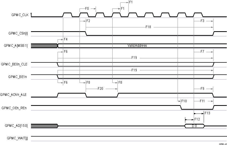
A. In GPMC_CSn[i], i is equal to 0,
1, 2 or 3.
B. In GPMC_WAIT[j], j is equal to 0
or 1.
Figure 6-39 GPMC and
NOR Flash — Synchronous Single Read (GPMCFCLKDIVIDER = 0) 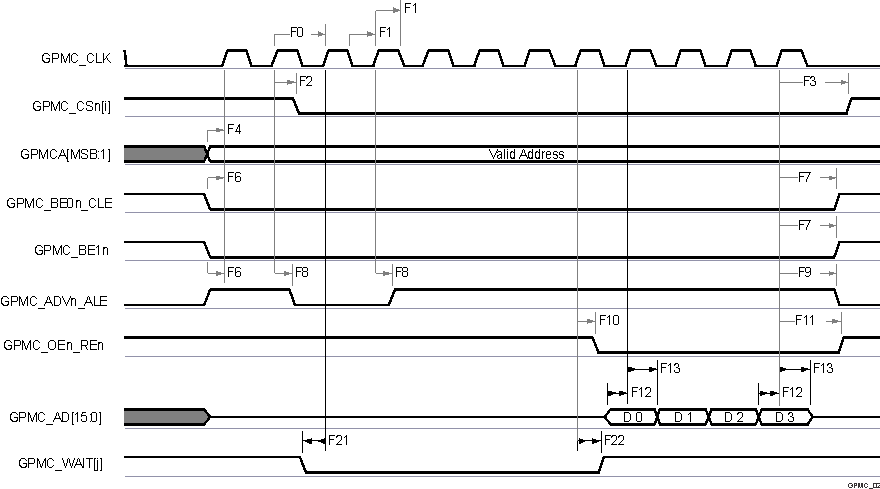
A. In GPMC_CSn[i], i is equal to 0,
1, 2 or 3.
B. In GPMC_WAIT[j], j is equal to 0
or 1.
Figure 6-40 GPMC and
NOR Flash — Synchronous Burst Read — 4x16–bit (GPMCFCLKDIVIDER = 0) 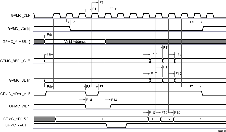
A. In GPMC_CSn[i], i is equal to 0,
1, 2 or 3.
B. In GPMC_WAIT[j], j is equal to 0
or 1.
Figure 6-41 GPMC and
NOR Flash—Synchronous Burst Write (GPMCFCLKDIVIDER = 0) 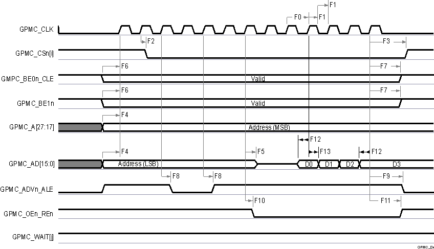
A. In GPMC_CSn[i], i is equal to 0,
1, 2 or 3.
B. In GPMC_WAIT[j], j is equal to 0
or 1.
Figure 6-42 GPMC and
Multiplexed NOR Flash — Synchronous Burst Read 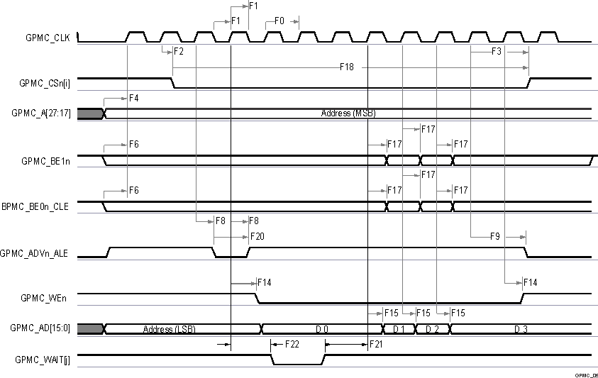
A. In GPMC_CSn[i], i is equal to 0,
1, 2 or 3.
B. In GPMC_WAIT[j], j is equal to 0
or 1.
Figure 6-43 GPMC and
Multiplexed NOR Flash — Synchronous Burst Write