JAJSL34G January 2021 – April 2024 AM6411 , AM6412 , AM6421 , AM6422 , AM6441 , AM6442
PRODUCTION DATA
- 1
- 1 特長
- 2 アプリケーション
- 3 概要
- 4 Device Comparison
-
5 Terminal Configuration and Functions
- 5.1 Pin Diagrams
- 5.2 Pin Attributes
- 5.3
Signal Descriptions
- 14
- 5.3.1 ADC
- 5.3.2 CPSW3G
- 5.3.3 CPTS
- 5.3.4 DDRSS
- 5.3.5 ECAP
- 5.3.6 Emulation and Debug
- 5.3.7 EPWM
- 5.3.8 EQEP
- 5.3.9 FSI
- 5.3.10 GPIO
- 5.3.11 GPMC
- 5.3.12 I2C
- 5.3.13 MCAN
- 5.3.14 MCSPI
- 5.3.15 MDIO
- 5.3.16 MMC
- 5.3.17 OSPI
- 5.3.18 Power Supply
- 5.3.19 PRU_ICSSG
- 5.3.20 Reserved
- 5.3.21 SERDES
- 5.3.22 System and Miscellaneous
- 5.3.23 TIMER
- 5.3.24 UART
- 5.3.25 USB
- 5.4 Pin Connectivity Requirements
-
6 Specifications
- 6.1 Absolute Maximum Ratings
- 6.2 ESD Ratings
- 6.3 Power-On Hours (POH)
- 6.4 Recommended Operating Conditions
- 6.5 Operating Performance Points
- 6.6 Power Consumption Summary
- 6.7
Electrical
Characteristics
- 6.7.1 I2C Open-Drain, and Fail-Safe (I2C OD FS) Electrical Characteristics
- 6.7.2 Fail-Safe Reset (FS RESET) Electrical Characteristics
- 6.7.3 High-Frequency Oscillator (HFOSC) Electrical Characteristics
- 6.7.4 eMMCPHY Electrical Characteristics
- 6.7.5 SDIO Electrical Characteristics
- 6.7.6 LVCMOS Electrical Characteristics
- 6.7.7 ADC12B Electrical Characteristics
- 6.7.8 USB2PHY Electrical Characteristics
- 6.7.9 SerDes PHY Electrical Characteristics
- 6.7.10 DDR Electrical Characteristics
- 6.8 VPP Specifications for One-Time Programmable (OTP) eFuses
- 6.9 Thermal Resistance Characteristics
- 6.10
Timing and Switching Characteristics
- 6.10.1 Timing Parameters and Information
- 6.10.2 Power Supply Requirements
- 6.10.3 System Timing
- 6.10.4 Clock Specifications
- 6.10.5
Peripherals
- 6.10.5.1 CPSW3G
- 6.10.5.2 DDRSS
- 6.10.5.3 ECAP
- 6.10.5.4 EPWM
- 6.10.5.5 EQEP
- 6.10.5.6 FSI
- 6.10.5.7 GPIO
- 6.10.5.8 GPMC
- 6.10.5.9 I2C
- 6.10.5.10 MCAN
- 6.10.5.11 MCSPI
- 6.10.5.12 MMCSD
- 6.10.5.13 CPTS
- 6.10.5.14 OSPI
- 6.10.5.15 PCIe
- 6.10.5.16
PRU_ICSSG
- 6.10.5.16.1 PRU_ICSSG Programmable Real-Time Unit (PRU)
- 6.10.5.16.2 PRU_ICSSG Pulse Width Modulation (PWM)
- 6.10.5.16.3 PRU_ICSSG Industrial Ethernet Peripheral (IEP)
- 6.10.5.16.4 PRU_ICSSG Universal Asynchronous Receiver Transmitter (UART)
- 6.10.5.16.5 PRU_ICSSG Enhanced Capture Peripheral (ECAP)
- 6.10.5.16.6 PRU_ICSSG RGMII, MII_RT, and Switch
- 6.10.5.17 Timers
- 6.10.5.18 UART
- 6.10.5.19 USB
- 6.10.6 Emulation and Debug
-
7 Detailed Description
- 7.1 Overview
- 7.2 Processor Subsystems
- 7.3 Accelerators and Coprocessors
- 7.4
Other Subsystems
- 7.4.1 PDMA Controller
- 7.4.2
Peripherals
- 7.4.2.1 ADC
- 7.4.2.2 DCC
- 7.4.2.3 Dual Date Rate (DDR) External Memory Interface (DDRSS)
- 7.4.2.4 ECAP
- 7.4.2.5 EPWM
- 7.4.2.6 ELM
- 7.4.2.7 ESM
- 7.4.2.8 GPIO
- 7.4.2.9 EQEP
- 7.4.2.10 General-Purpose Memory Controller (GPMC)
- 7.4.2.11 I2C
- 7.4.2.12 MCAN
- 7.4.2.13 MCRC Controller
- 7.4.2.14 MCSPI
- 7.4.2.15 MMCSD
- 7.4.2.16 OSPI
- 7.4.2.17 Peripheral Component Interconnect Express (PCIe)
- 7.4.2.18 Serializer/Deserializer (SerDes) PHY
- 7.4.2.19 Real Time Interrupt (RTI/WWDT)
- 7.4.2.20 Dual Mode Timer (DMTIMER)
- 7.4.2.21 UART
- 7.4.2.22 Universal Serial Bus Subsystem (USBSS)
-
8 Applications,
Implementation, and Layout
- 8.1 Device Connection and Layout Fundamentals
- 8.2 Peripheral- and Interface-Specific Design Information
- 8.3 Clock Routing Guidelines
- 9 Device and Documentation Support
- 10Revision History
- 11Mechanical, Packaging, and Orderable Information
パッケージ・オプション
デバイスごとのパッケージ図は、PDF版データシートをご参照ください。
メカニカル・データ(パッケージ|ピン)
- ALV|441
サーマルパッド・メカニカル・データ
発注情報
6.10.5.8.3 GPMC and NAND Flash — Asynchronous Mode
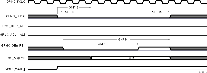
Table 6-58 and Table 6-59 present timing requirements and switching characteristics for GPMC and NAND Flash — Asynchronous Mode.
Table 6-58 GPMC and NAND Flash Timing Requirements – Asynchronous Mode see Figure 6-52
| NO. | PARAMETER | DESCRIPTION | MODE(4) | MIN | MAX | UNIT |
|---|---|---|---|---|---|---|
| 133 MHz | ||||||
| GNF12(1) | tacc(d) | Access time, input data GPMC_AD[15:0](3) | div_by_1_mode; GPMC_FCLK_MUX; TIMEPARAGRANULARITY_X1 |
J(2) | ns | |
(1) The GNF12 parameter illustrates the amount of time required to
internally sample input data. It is expressed in number of GPMC functional clock
cycles. From start of the read cycle and after GNF12 functional clock cycles,
input data is internally sampled by the active functional clock edge. The GNF12
value must be stored inside AccessTime register bit field.
(2) J =
AccessTime × (TimeParaGranularity + 1) × GPMC_FCLK(3)
(3) GPMC_FCLK is general-purpose memory controller internal
functional clock period in ns.
(4) For
div_by_1_mode:
For GPMC_FCLK_MUX:
For TIMEPARAGRANULARITY_X1:
- GPMC_CONFIG1_i Register:
GPMCFCLKDIVIDER = 0h:
- GPMC_CLK frequency = GPMC_FCLK frequency
For GPMC_FCLK_MUX:
- CTRLMMR_GPMC_CLKSEL[1-0] CLK_SEL = 00 = CPSWHSDIV_CLKOUT3 = 2000/15 = 133.33 MHz
For TIMEPARAGRANULARITY_X1:
- GPMC_CONFIG1_i Register: TIMEPARAGRANULARITY = 0h = x1 latencies (affecting RD/WRCYCLETIME, RD/WRACCESSTIME, PAGEBURSTACCESSTIME, CSONTIME, CSRD/WROFFTIME, ADVONTIME, ADVRD/WROFFTIME, OEONTIME, OEOFFTIME, WEONTIME, WEOFFTIME, CYCLE2CYCLEDELAY, BUSTURNAROUND, TIMEOUTSTARTVALUE, WRDATAONADMUXBUS)
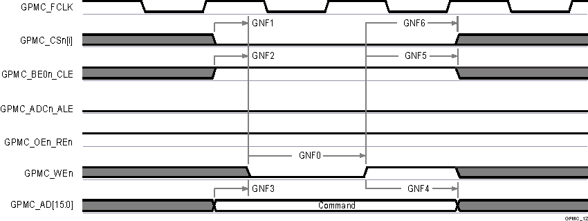
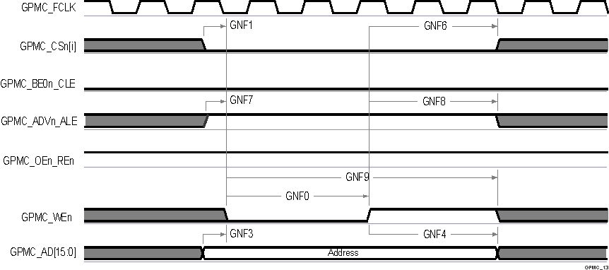
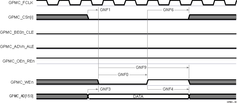
Table 6-59 GPMC and NAND Flash Switching Characteristics – Asynchronous Mode see Figure 6-50,
Figure 6-51,
Figure 6-52 and
Figure 6-53
| NO. | PARAMETER | MODE(4) | MIN | MAX | UNIT | |
|---|---|---|---|---|---|---|
| GNF0 | tw(wenV) | Pulse duration, output write enable GPMC_WEn valid | div_by_1_mode; GPMC_FCLK_MUX; TIMEPARAGRANULARITY_X1 |
A | ns | |
| GNF1 | td(csnV-wenV) | Delay time, output chip select GPMC_CSn[i](2) valid to output write enable GPMC_WEn valid | div_by_1_mode; GPMC_FCLK_MUX; TIMEPARAGRANULARITY_X1 |
B - 2 | B + 2 | ns |
| GNF2 | tw(cleH-wenV) | Delay time, output lower-byte enable and command latch enable GPMC_BE0n_CLE high to output write enable GPMC_WEn valid | div_by_1_mode; GPMC_FCLK_MUX; TIMEPARAGRANULARITY_X1 |
C - 2 | C + 2 | ns |
| GNF3 | tw(wenV-dV) | Delay time, output data GPMC_AD[15:0] valid to output write enable GPMC_WEn valid | div_by_1_mode; GPMC_FCLK_MUX; TIMEPARAGRANULARITY_X1 |
D - 2 | D + 2 | ns |
| GNF4 | tw(wenIV-dIV) | Delay time, output write enable GPMC_WEn invalid to output data GPMC_AD[15:0] invalid | div_by_1_mode; GPMC_FCLK_MUX; TIMEPARAGRANULARITY_X1 |
E - 2 | E + 2 | ns |
| GNF5 | tw(wenIV-cleIV) | Delay time, output write enable GPMC_WEn invalid to output lower-byte enable and command latch enable GPMC_BE0n_CLE invalid | div_by_1_mode; GPMC_FCLK_MUX; TIMEPARAGRANULARITY_X1 |
F - 2 | F + 2 | ns |
| GNF6 | tw(wenIV-CSn[i]V) | Delay time, output write enable GPMC_WEn invalid to output chip select GPMC_CSn[i](2) invalid | div_by_1_mode; GPMC_FCLK_MUX; TIMEPARAGRANULARITY_X1 |
G - 2 | G + 2 | ns |
| GNF7 | tw(aleH-wenV) | Delay time, output address valid and address latch enable GPMC_ADVn_ALE high to output write enable GPMC_WEn valid | div_by_1_mode; GPMC_FCLK_MUX; TIMEPARAGRANULARITY_X1 |
C - 2 | C + 2 | ns |
| GNF8 | tw(wenIV-aleIV) | Delay time, output write enable GPMC_WEn invalid to output address valid and address latch enable GPMC_ADVn_ALE invalid | div_by_1_mode; GPMC_FCLK_MUX; TIMEPARAGRANULARITY_X1 |
F - 2 | F + 2 | ns |
| GNF9 | tc(wen) | Cycle time, write | div_by_1_mode; GPMC_FCLK_MUX; TIMEPARAGRANULARITY_X1 |
H | ns | |
| GNF10 | td(csnV-oenV) | Delay time, output chip select GPMC_CSn[i](2) valid to output enable GPMC_OEn_REn valid | div_by_1_mode; GPMC_FCLK_MUX; TIMEPARAGRANULARITY_X1 |
I - 2 | I + 2 | ns |
| GNF13 | tw(oenV) | Pulse duration, output enable GPMC_OEn_REn valid | div_by_1_mode; GPMC_FCLK_MUX; TIMEPARAGRANULARITY_X1 |
K | ns | |
| GNF14 | tc(oen) | Cycle time, read | div_by_1_mode; GPMC_FCLK_MUX; TIMEPARAGRANULARITY_X1 |
L | ns | |
| GNF15 | tw(oenIV-CSn[i]V) | Delay time, output enable GPMC_OEn_REn invalid to output chip select GPMC_CSn[i](2) invalid | div_by_1_mode; GPMC_FCLK_MUX; TIMEPARAGRANULARITY_X1 |
M - 2 | M + 2 | ns |
(2) In GPMC_CSn[i], i is equal to 0, 1, 2 or 3.
(3) GPMC_FCLK is general-purpose memory controller internal
functional clock period in ns.
(4) For div_by_1_mode:
For GPMC_FCLK_MUX:
For TIMEPARAGRANULARITY_X1:
- GPMC_CONFIG1_i Register:
GPMCFCLKDIVIDER = 0h:
- GPMC_CLK frequency = GPMC_FCLK frequency
For GPMC_FCLK_MUX:
- CTRLMMR_GPMC_CLKSEL[1-0] CLK_SEL = 00 = CPSWHSDIV_CLKOUT3 = 2000/15 = 133.33 MHz
For TIMEPARAGRANULARITY_X1:
- GPMC_CONFIG1_i Register: TIMEPARAGRANULARITY = 0h = x1 latencies (affecting RD/WRCYCLETIME, RD/WRACCESSTIME, PAGEBURSTACCESSTIME, CSONTIME, CSRD/WROFFTIME, ADVONTIME, ADVRD/WROFFTIME, OEONTIME, OEOFFTIME, WEONTIME, WEOFFTIME, CYCLE2CYCLEDELAY, BUSTURNAROUND, TIMEOUTSTARTVALUE, WRDATAONADMUXBUS)

A. In GPMC_CSn[i], i is equal to 0,
1, 2 or 3.
Figure 6-50 GPMC and
NAND Flash — Command Latch Cycle
A. In GPMC_CSn[i], i is equal to 0,
1, 2 or 3.
Figure 6-51 GPMC and
NAND Flash — Address Latch Cycle
A. GNF12 parameter illustrates
amount of time required to internally sample input data. It is expressed in
number of GPMC functional clock cycles. From start of read cycle and after GNF12
functional clock cycles, input data will be internally sampled by active
functional clock edge. GNF12 value must be stored inside AccessTime register
bits field.
B. GPMC_FCLK is an internal clock
(GPMC functional clock) not provided externally.
C. In GPMC_CSn[i], i is equal to 0,
1, 2 or 3. In GPMC_WAIT[j], j is equal to 0 or 1.
Figure 6-52 GPMC and
NAND Flash — Data Read Cycle 
A. `In GPMC_CSn[i], i is equal to
0, 1, 2 or 3.
Figure 6-53 GPMC and
NAND Flash — Data Write Cycle