JAJSIU4B April 2020 – June 2022 AMC1300B-Q1
PRODUCTION DATA
- 1 特長
- 2 アプリケーション
- 3 概要
- 4 Revision History
- 5 Pin Configuration and Functions
-
6 Specifications
- 6.1 Absolute Maximum Ratings
- 6.2 ESD Ratings
- 6.3 Recommended Operating Conditions
- 6.4 Thermal Information
- 6.5 Power Ratings
- 6.6 Insulation Specifications
- 6.7 Safety-Related Certifications
- 6.8 Safety Limiting Values
- 6.9 Electrical Characteristics
- 6.10 Switching Characteristics
- 6.11 Timing Diagram
- 6.12 Insulation Characteristics Curves
- 6.13 Typical Characteristics
- 7 Detailed Description
- 8 Application and Implementation
- 9 Power Supply Recommendations
- 10Layout
- 11Device and Documentation Support
- 12Mechanical, Packaging, and Orderable Information
5 Pin Configuration and Functions
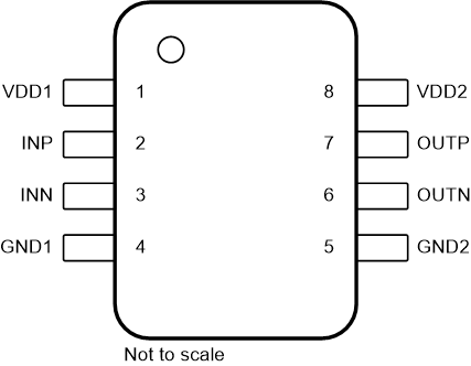
 Figure 5-1
DWV Package,8-Pin SOIC(Top View)
Table 5-1 Pin Functions
| PIN | TYPE | DESCRIPTION | |
|---|---|---|---|
| NO. | NAME | ||
| 1 | VDD1 | High-side power | High-side power supply.(1) |
| 2 | INP | Analog input | Noninverting analog input. Either INP or INN must have a DC current path to GND1 to define the common-mode input voltage.(2) |
| 3 | INN | Analog input | Inverting analog input. Either INP or INN must have a DC current path to GND1 to define the common-mode input voltage.(2) |
| 4 | GND1 | High-side ground | High-side analog ground. |
| 5 | GND2 | Low-side ground | Low-side analog ground. |
| 6 | OUTN | Analog output | Inverting analog output. |
| 7 | OUTP | Analog output | Noninverting analog output. |
| 8 | VDD2 | Low-side power | Low-side power supply.(1) |
(1) See the
Section 9 section for power-supply decoupling
recommendations.
(2) See the Section 10 section for details.