JAJSP46A May 2023 – September 2023 AMC130M03
PRODUCTION DATA
- 1
- 1 特長
- 2 アプリケーション
- 3 概要
- 4 Revision History
- 5 Pin Configuration and Functions
-
6 Specifications
- 6.1 Absolute Maximum Ratings
- 6.2 ESD Ratings
- 6.3 Recommended Operating Conditions
- 6.4 Thermal Information
- 6.5 Insulation Specifications
- 6.6 Safety-Related Certifications
- 6.7 Safety Limiting Values
- 6.8 Electrical Characteristics
- 6.9 Timing Requirements
- 6.10 Switching Characteristics
- 6.11 Timing Diagrams
- 6.12 Typical Characteristics
- 7 Parameter Measurement Information
-
8 Detailed Description
- 8.1 Overview
- 8.2 Functional Block Diagram
- 8.3
Feature Description
- 8.3.1 Isolated DC/DC Converter
- 8.3.2 High-Side Current Drive Capability
- 8.3.3 Isolation Channel Signal Transmission
- 8.3.4 Input ESD Protection Circuitry
- 8.3.5 Input Multiplexer
- 8.3.6 Programmable Gain Amplifier (PGA)
- 8.3.7 Voltage Reference
- 8.3.8 Internal Test Signals
- 8.3.9 Clocking and Power Modes
- 8.3.10 ΔΣ Modulator
- 8.3.11 Digital Filter
- 8.3.12 Channel Phase Calibration
- 8.3.13 Calibration Registers
- 8.3.14 Register Map CRC
- 8.3.15 Temperature Sensor
- 8.3.16 General-Purpose Digital Output (GPO)
- 8.4 Device Functional Modes
- 8.5
Programming
- 8.5.1
Serial Interface
- 8.5.1.1 Chip Select (CS)
- 8.5.1.2 Serial Data Clock (SCLK)
- 8.5.1.3 Serial Data Input (DIN)
- 8.5.1.4 Serial Data Output (DOUT)
- 8.5.1.5 Data Ready (DRDY)
- 8.5.1.6 Conversion Synchronization or System Reset (SYNC/RESET)
- 8.5.1.7 SPI Communication Frames
- 8.5.1.8 SPI Communication Words
- 8.5.1.9 Short SPI Frames
- 8.5.1.10 Communication Cyclic Redundancy Check (CRC)
- 8.5.1.11 SPI Timeout
- 8.5.2 ADC Conversion Data Format
- 8.5.3 Commands
- 8.5.4 ADC Output Buffer and FIFO Buffer
- 8.5.5 Collecting Data for the First Time or After a Pause in Data Collection
- 8.5.1
Serial Interface
- 8.6 AMC130M03 Registers
- 9 Application and Implementation
- 10Device and Documentation Support
- 11Mechanical, Packaging, and Orderable Information
8.3.3 Isolation Channel Signal Transmission
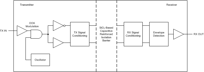
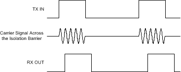
The AMC130M03 uses an on-off keying (OOK) modulation scheme to transmit the modulator output bitstream across the capacitive SiO2-based isolation barrier. After transmission across the isolation barrier, the modulator output bitstream is decimated using the sinc filter to reconstruct the ADC conversion data, and is then transferred to the digital control so that the data are accessible through the SPI interface. Figure 8-1 depicts the block diagram of an isolation channel. The transmitter modulates the bitstream at TX IN with an internally generated, 480-MHz carrier and sends a burst across the isolation barrier to represent a digital one and sends a no signal to represent the digital zero. The receiver demodulates the signal after advanced signal conditioning and produces the output. The symmetrical design of each isolation channel improves the common-mode transient immunity (CMTI) performance and reduces the radiated emissions caused by the high-frequency carrier.
 Figure 8-1 Block
Diagram of an Isolation Channel
Figure 8-1 Block
Diagram of an Isolation ChannelFigure 8-2 shows the concept of the on-off keying scheme.
 Figure 8-2 OOK-Based
Modulation Scheme