JAJSR83 September 2023 AMC131M02
PRODUCTION DATA
- 1
- 1 特長
- 2 アプリケーション
- 3 概要
- 4 Revision History
- 5 Pin Configuration and Functions
-
6 Specifications
- 6.1 Absolute Maximum Ratings
- 6.2 ESD Ratings
- 6.3 Recommended Operating Conditions
- 6.4 Thermal Information
- 6.5 Insulation Specifications
- 6.6 Safety-Related Certifications
- 6.7 Safety Limiting Values
- 6.8 Electrical Characteristics
- 6.9 Timing Requirements
- 6.10 Switching Characteristics
- 6.11 Timing Diagrams
- 6.12 Typical Characteristics
- 7 Parameter Measurement Information
-
8 Detailed Description
- 8.1 Overview
- 8.2 Functional Block Diagram
- 8.3
Feature Description
- 8.3.1 Isolated DC/DC Converter
- 8.3.2 High-Side Current Drive Capability
- 8.3.3 Isolation Channel Signal Transmission
- 8.3.4 Input ESD Protection Circuitry
- 8.3.5 Input Multiplexer
- 8.3.6 Programmable Gain Amplifier (PGA)
- 8.3.7 Voltage Reference
- 8.3.8 Internal Test Signals
- 8.3.9 Clocking and Power Modes
- 8.3.10 ΔΣ Modulator
- 8.3.11 Digital Filter
- 8.3.12 Channel Phase Calibration
- 8.3.13 Calibration Registers
- 8.3.14 Register Map CRC
- 8.3.15 General-Purpose Digital Output (GPO)
- 8.4 Device Functional Modes
- 8.5
Programming
- 8.5.1
Serial Interface
- 8.5.1.1 Chip Select (CS)
- 8.5.1.2 Serial Data Clock (SCLK)
- 8.5.1.3 Serial Data Input (DIN)
- 8.5.1.4 Serial Data Output (DOUT)
- 8.5.1.5 Data Ready (DRDY)
- 8.5.1.6 Conversion Synchronization or System Reset (SYNC/RESET)
- 8.5.1.7 SPI Communication Frames
- 8.5.1.8 SPI Communication Words
- 8.5.1.9 Short SPI Frames
- 8.5.1.10 Communication Cyclic Redundancy Check (CRC)
- 8.5.1.11 SPI Timeout
- 8.5.2 ADC Conversion Data
- 8.5.3 Commands
- 8.5.4 ADC Output Buffer and FIFO Buffer
- 8.5.5 Collecting Data for the First Time or After a Pause in Data Collection
- 8.5.1
Serial Interface
- 8.6 AMC131M02 Registers
- 9 Application and Implementation
- 10Device and Documentation Support
- 11Mechanical, Packaging, and Orderable Information
8.3.13 Calibration Registers
The calibration registers allow for automatic computation of calibrated ADC conversion results from preprogrammed values. The host can rely on the device to automatically correct for system gain and offset after the error correction terms are programmed into the corresponding device registers. The measured calibration coefficients must be stored in external nonvolatile memory and programmed into the registers each time the AMC131M02 powers up because the AMC131M02 registers are volatile.
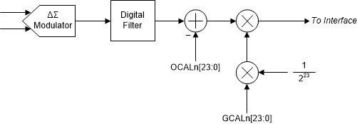
The offset calibration registers are used to correct for system offset error, otherwise known as zero error. Offset error corresponds to the ADC output when the input to the system is zero. The AMC131M02 corrects for offset errors by subtracting the contents of the OCALn[23:0] register bits in the CHn_OCAL_MSB and CHn_OCAL_LSB registers from the conversion result for that channel before being output. There are separate CHn_OCAL_MSB and CHnOCAL_LSB registers for each channel, which allows separate offset calibration coefficients to be programmed for each channel. The contents of the OCALn[23:0] bits are interpreted by the device as 24-bit, two's-complement values.
The gain calibration registers are used to correct for system gain error. Gain error corresponds to the deviation of gain of the system from the ideal value. The AMC131M02 corrects for gain errors by multiplying the ADC conversion result by the value given by the contents of the GCALn[23:0] register bits in the CHn_GCAL_MSB and CHn_GCAL_LSB registers before being output. There are separate CHn_GCAL_MSB and CHn_GCAL_LSB registers for each channel, which allows separate gain calibration coefficients to be programmed for each channel. The contents of the GCALn[23:0] bits are interpreted by the device as 24-bit unsigned values corresponding to linear steps ranging from gains of 0 to 2 – (1 / 223). Table 8-7 describes the relationship between the GCALn[23:0] bit values and the gain calibration factor.
| GCALn[23:0] VALUE | GAIN CALIBRATION FACTOR |
|---|---|
| 000000h | 0 |
| 000001h | 1.19 × 10⁻⁷ |
| 800000h | 1 |
| FFFFFEh | 2 – 2.38 × 10⁻⁷ |
| FFFFFFh | 2 – 1.19 × 10⁻⁷ |
The calibration registers do not need to be enabled because these registers are always in use. The OCALn[23:0] bits have a default value of 000000h resulting in no offset correction. Similarly, the GCALn[23:0] bits default to 800000h resulting in a gain calibration factor of 1.
Figure 8-14 shows a block diagram illustrating the mechanics of the calibration registers on one channel of the AMC131M02.
 Figure 8-14 Calibration Block Diagram