JAJSR83 September   2023 AMC131M02

PRODUCTION DATA  

  1.   1
  2. 特長
  3. アプリケーション
  4. 概要
  5. Revision History
  6. Pin Configuration and Functions
  7. Specifications
    1. 6.1  Absolute Maximum Ratings
    2. 6.2  ESD Ratings
    3. 6.3  Recommended Operating Conditions
    4. 6.4  Thermal Information
    5. 6.5  Insulation Specifications
    6. 6.6  Safety-Related Certifications
    7. 6.7  Safety Limiting Values
    8. 6.8  Electrical Characteristics
    9. 6.9  Timing Requirements
    10. 6.10 Switching Characteristics
    11. 6.11 Timing Diagrams
    12. 6.12 Typical Characteristics
  8. Parameter Measurement Information
    1. 7.1 Noise Measurements
  9. Detailed Description
    1. 8.1 Overview
    2. 8.2 Functional Block Diagram
    3. 8.3 Feature Description
      1. 8.3.1  Isolated DC/DC Converter
        1. 8.3.1.1 DC/DC Converter Failure Detection
      2. 8.3.2  High-Side Current Drive Capability
      3. 8.3.3  Isolation Channel Signal Transmission
      4. 8.3.4  Input ESD Protection Circuitry
      5. 8.3.5  Input Multiplexer
      6. 8.3.6  Programmable Gain Amplifier (PGA)
      7. 8.3.7  Voltage Reference
      8. 8.3.8  Internal Test Signals
      9. 8.3.9  Clocking and Power Modes
      10. 8.3.10 ΔΣ Modulator
      11. 8.3.11 Digital Filter
        1. 8.3.11.1 Digital Filter Implementation
          1. 8.3.11.1.1 Fast-Settling Filter
          2. 8.3.11.1.2 SINC3 and SINC3 + SINC1 Filter
        2. 8.3.11.2 Digital Filter Characteristic
      12. 8.3.12 Channel Phase Calibration
      13. 8.3.13 Calibration Registers
      14. 8.3.14 Register Map CRC
      15. 8.3.15 General-Purpose Digital Output (GPO)
    4. 8.4 Device Functional Modes
      1. 8.4.1 Power-Up and Reset
        1. 8.4.1.1 Power-On Reset
        2. 8.4.1.2 SYNC/RESET Pin
        3. 8.4.1.3 RESET Command
      2. 8.4.2 Start-Up Behavior After Power-Up
      3. 8.4.3 Start-Up Behavior After a Pin Reset or RESET Command
      4. 8.4.4 Start-Up Behavior After a Pause in CLKIN
      5. 8.4.5 Synchronization
      6. 8.4.6 Conversion Modes
        1. 8.4.6.1 Continuous-Conversion Mode
        2. 8.4.6.2 Global-Chop Mode
      7. 8.4.7 Power Modes
      8. 8.4.8 Standby Mode
    5. 8.5 Programming
      1. 8.5.1 Serial Interface
        1. 8.5.1.1  Chip Select (CS)
        2. 8.5.1.2  Serial Data Clock (SCLK)
        3. 8.5.1.3  Serial Data Input (DIN)
        4. 8.5.1.4  Serial Data Output (DOUT)
        5. 8.5.1.5  Data Ready (DRDY)
        6. 8.5.1.6  Conversion Synchronization or System Reset (SYNC/RESET)
        7. 8.5.1.7  SPI Communication Frames
        8. 8.5.1.8  SPI Communication Words
        9. 8.5.1.9  Short SPI Frames
        10. 8.5.1.10 Communication Cyclic Redundancy Check (CRC)
        11. 8.5.1.11 SPI Timeout
      2. 8.5.2 ADC Conversion Data
      3. 8.5.3 Commands
        1. 8.5.3.1 NULL (0000 0000 0000 0000)
        2. 8.5.3.2 RESET (0000 0000 0001 0001)
        3. 8.5.3.3 STANDBY (0000 0000 0010 0010)
        4. 8.5.3.4 WAKEUP (0000 0000 0011 0011)
        5. 8.5.3.5 LOCK (0000 0101 0101 0101)
        6. 8.5.3.6 UNLOCK (0000 0110 0101 0101)
        7. 8.5.3.7 RREG (101a aaaa annn nnnn)
          1. 8.5.3.7.1 Reading a Single Register
          2. 8.5.3.7.2 Reading Multiple Registers
        8. 8.5.3.8 WREG (011a aaaa annn nnnn)
      4. 8.5.4 ADC Output Buffer and FIFO Buffer
      5. 8.5.5 Collecting Data for the First Time or After a Pause in Data Collection
    6. 8.6 AMC131M02 Registers
  10. Application and Implementation
    1. 9.1 Application Information
      1. 9.1.1 Unused Inputs and Outputs
      2. 9.1.2 Antialiasing
      3. 9.1.3 Minimum Interface Connections
      4. 9.1.4 Multiple Device Configuration
      5. 9.1.5 Calibration
      6. 9.1.6 Troubleshooting
    2. 9.2 Typical Application
      1. 9.2.1 Design Requirements
      2. 9.2.2 Detailed Design Procedure
        1. 9.2.2.1 Voltage Measurement
        2. 9.2.2.2 Current Shunt Measurement
      3. 9.2.3 Application Curves
    3. 9.3 Power Supply Recommendations
    4. 9.4 Layout
      1. 9.4.1 Layout Guidelines
      2. 9.4.2 Layout Example
  11. 10Device and Documentation Support
    1. 10.1 Documentation Support
      1. 10.1.1 Related Documentation
    2. 10.2 ドキュメントの更新通知を受け取る方法
    3. 10.3 サポート・リソース
    4. 10.4 Trademarks
    5. 10.5 静電気放電に関する注意事項
    6. 10.6 用語集
  12. 11Mechanical, Packaging, and Orderable Information

パッケージ・オプション

メカニカル・データ(パッケージ|ピン)
サーマルパッド・メカニカル・データ
発注情報

Typical Characteristics

for channel 0 at TA = 25°C, DVDD = 3.3 V, fCLKIN = 8.192 MHz, data rate = 4 kSPS (OSR = 1024 and clock divider NDIV = 2), high-resolution mode, with all channels enabled, global-chop mode disabled, and gain = 1 (unless otherwise noted)
GUID-20230802-SS0I-HWDM-H067-PWJKBPBWCD5R-low.png
 
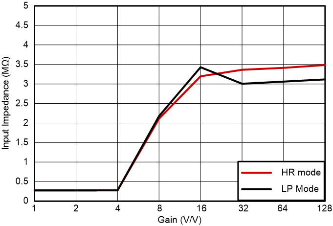
Figure 6-4 Input Impedance vs Gain
GUID-20230802-SS0I-DHLN-9NJC-FRMZS5LGFP4Q-low.png
 
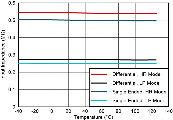
Figure 6-6 Input Impedance vs Temperature
GUID-20230902-SS0I-TZK6-SBFL-ZPQ4RXNC7DGF-low.svg
 
Figure 6-8 Offset Error vs Gain
GUID-20230804-SS0I-2K5N-3S7G-MV8VT2LMQSP9-low.png
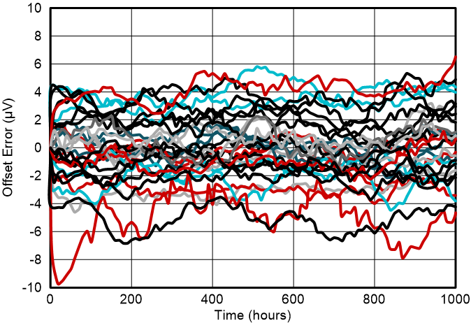
30 units, 85°C
Figure 6-10 Offset Error vs Time
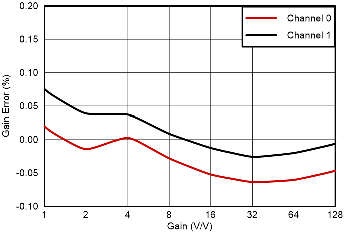
GUID-20230902-SS0I-Z50T-L6ZQ-PDXZ8HKQKZWD-low.png
 
Figure 6-12 Gain Error vs Gain
GUID-20230902-SS0I-VCCT-28LN-HZJKNDV3WDGJ-low.svg
 
Figure 6-14 Dynamic Range vs Gain
GUID-20230802-SS0I-7WF8-3KHZ-N9NSLLRHNZX0-low.svg
Averaged FFT, frequency bin width equals 1 Hz
Figure 6-16 Frequency Spectrum With 50-Hz Input Signal
GUID-20230802-SS0I-PRMM-DX9M-DFTS59FGSGLM-low.svg
 
Figure 6-18 DVDD Current vs CLKIN Frequency
GUID-20230802-SS0I-CH3F-KGP9-J3H0JT5B9SXM-low.svg
 
Figure 6-20 HLDO Output Voltage vs Temperature
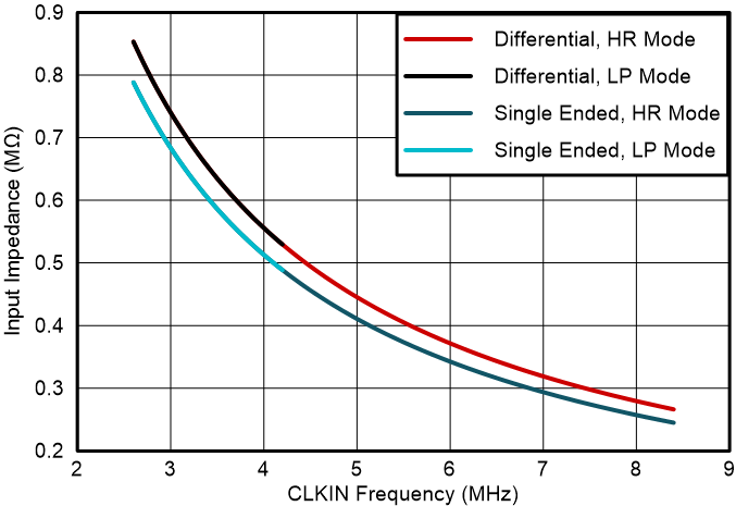
GUID-20230802-SS0I-4V42-WC7P-QZ2DWSDVZXF0-low.png
 
Figure 6-5 Input Impedance vs CLKIN Frequency
GUID-20230802-SS0I-VPP2-CH92-ZH9DVHJT4ZBK-low.svg
 
Figure 6-7 Input Current vs Differential Input Voltage
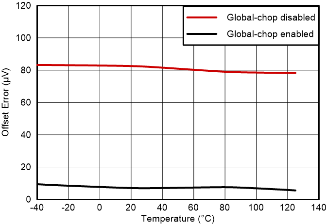
GUID-20230804-SS0I-HKKV-KP4M-SMQMLPPVS8LN-low.png
 
Figure 6-9 Offset Error vs Temperature
GUID-20230804-SS0I-BHVZ-6V7L-JQNRBQ5CMJQC-low.svg
30 units, 85°C
Figure 6-11 Gain Error vs Time
GUID-20230807-SS0I-H04G-1GNP-GMCRMJPSZ6MX-low.svg
 
Figure 6-13 Gain Error vs Temperature
GUID-20230804-SS0I-907F-LHPT-RSC8RMVV24LL-low.svg
 
Figure 6-15 Dynamic Range vs OSR
GUID-20230802-SS0I-SCHT-LBZH-BFB5X8SDWSKF-low.svg
Averaged FFT, frequency bin width equals 1 Hz
Figure 6-17 Noise Spectral Density vs Frequency
GUID-20230802-SS0I-C3MQ-MP0S-4X065JZKJD7N-low.png
 
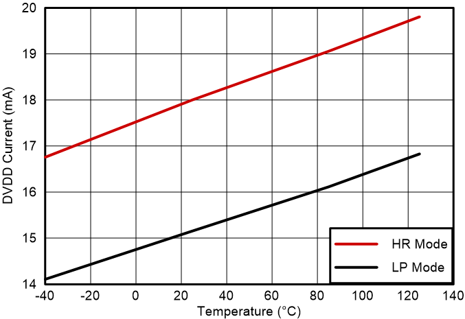
Figure 6-19 DVDD Current vs Temperature
GUID-20230802-SS0I-TRWS-M5W0-NS8HDLQFCK7V-low.svg
 
Figure 6-21 HLDO Output Voltage vs Load Current