JAJSNB2D November 2021 – September 2024 AWR2944
PRODUCTION DATA
- 1
- 1 特長
- 2 アプリケーション
- 3 概要
- 4 Device Comparison
- 5 Pin Configurations and Functions
-
6 Specifications
- 6.1 Absolute Maximum Ratings
- 6.2 ESD Ratings
- 6.3 Power-On Hours (POH)
- 6.4 Recommended Operating Conditions
- 6.5 VPP Specifications for One-Time Programmable (OTP) eFuses
- 6.6 Power Supply Specifications
- 6.7 Power Consumption Summary
- 6.8 RF Specifications
- 6.9 Thermal Resistance Characteristics
- 6.10 Power Supply Sequencing and Reset Timing
- 6.11 Input Clocks and Oscillators
- 6.12
Peripheral Information
- 6.12.1
QSPI Flash Memory Peripheral
- 6.12.1.1 QSPI Timing Conditions
- 6.12.1.2 QSPI Timing Requirements #GUID-CD30070D-F132-4A2C-92CD-5AA96AE70B94/GUID-97D19708-D87E-443B-9ADF-1760CFEF6F4C #GUID-CD30070D-F132-4A2C-92CD-5AA96AE70B94/GUID-0A61EEC9-2B95-4C27-B219-18D27C8F9430
- 6.12.1.3 QSPI Switching Characteristics #GUID-20B35D26-AFE6-451C-B9E9-B3F2FA08097C/T4362547-64 #GUID-20B35D26-AFE6-451C-B9E9-B3F2FA08097C/T4362547-65
- 6.12.2
Multibuffered / Standard Serial Peripheral Interface (MibSPI)
- 6.12.2.1 MibSPI Peripheral Description
- 6.12.2.2
MibSPI Transmit and Receive RAM Organization
- 6.12.2.2.1 SPI Timing Conditions
- 6.12.2.2.2 SPI Controller Mode Switching Parameters (CLOCK PHASE = 0, SPICLK = output, SPISIMO = output, and SPISOMI = input) #GUID-20BA2ACF-4FC2-43F6-960F-1A4CA56E65A6/T4362547-236 #GUID-20BA2ACF-4FC2-43F6-960F-1A4CA56E65A6/T4362547-237 #GUID-20BA2ACF-4FC2-43F6-960F-1A4CA56E65A6/T4362547-238
- 6.12.2.2.3 SPI Controller Mode Switching Parameters (CLOCK PHASE = 1, SPICLK = output, SPISIMO = output, and SPISOMI = input) #GUID-517E5284-3345-461F-B07F-EB95741B1272/T4362547-244 #GUID-517E5284-3345-461F-B07F-EB95741B1272/T4362547-245 #GUID-517E5284-3345-461F-B07F-EB95741B1272/T4362547-246
- 6.12.2.3 SPI Peripheral Mode I/O Timings
- 6.12.3
Ethernet Switch (RGMII/RMII/MII)
Peripheral
- 6.12.3.1 RGMII Timing Conditions
- 6.12.3.2 RGMII Transmit Clock Switching Characteristics
- 6.12.3.3 RGMII Transmit Data and Control Switching Characteristics
- 6.12.3.4 RGMII Receive Clock Timing Requirements
- 6.12.3.5 RGMII Receive Data and Control Timing Requirements
- 6.12.3.6 RMII Transmit Clock Switching Characteristics
- 6.12.3.7 RMII Transmit Data and Control Switching Characteristics
- 6.12.3.8 RMII Receive Clock Timing Requirements
- 6.12.3.9 RMII Receive Data and Control Timing Requirements
- 6.12.3.10 MII Transmit Switching Characteristics
- 6.12.3.11 MII Receive Clock Timing Requirements
- 6.12.3.12 MII Receive Timing Requirements
- 6.12.3.13 MII Transmit Clock Timing Requirements
- 6.12.3.14 MDIO Interface Timings
- 6.12.4 LVDS/Aurora Instrumentation and Measurement Peripheral
- 6.12.5 UART Peripheral
- 6.12.6 Inter-Integrated Circuit Interface (I2C)
- 6.12.7 Controller Area Network - Flexible Data-rate (CAN-FD)
- 6.12.8 CSI2 Receiver Peripheral
- 6.12.9 Enhanced Pulse-Width Modulator (ePWM)
- 6.12.10 General-Purpose Input/Output
- 6.12.1
QSPI Flash Memory Peripheral
- 6.13 Emulation and Debug
- 7 Detailed Description
- 8 Monitoring and Diagnostics
- 9 Applications, Implementation, and Layout
- 10デバイスおよびドキュメントのサポート
- 11Revision History
- 12Mechanical, Packaging, and Orderable Information
7.3.1.1 RF Clock Subsystem
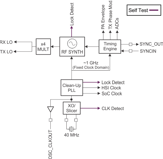
The device clock subsystem generates 76 to 81 GHz from an input reference of 40 MHz crystal. It has a built-in oscillator circuit followed by an Analog PLL and a RF synthesizer circuit. The output of the RF synthesizer is then processed by an x4 multiplier to create the required frequency in the 76 to 81 GHz spectrum. The RF synthesizer output can be modulated by the timing engine block to create the required waveforms for effective sensor operation or it can input a fixed signal of 1GHz directly from APLL.
The Analog PLL also provides a reference clock for the host processor after system wakeup.
The clock subsystem also has built-in mechanisms for detecting the presence of a crystal and monitoring the quality of the generated clock.
Figure 7-2 describes the clock subsystem.
 Figure 7-2 RF Clock Subsystem