JAJSIZ9D April 2020 – January 2022 AWR6443 , AWR6843
PRODUCTION DATA
- 1 特長
- 2 アプリケーション
- 3 概要
- 4 機能ブロック図
- 5 Device Comparison
- 6 Terminal Configuration and Functions
-
7 Specifications
- 7.1 Absolute Maximum Ratings
- 7.2 ESD Ratings
- 7.3 Power-On Hours (POH)
- 7.4 Recommended Operating Conditions
- 7.5 Power Supply Specifications
- 7.6 Power Consumption Summary
- 7.7 RF Specification
- 7.8 CPU Specifications
- 7.9 Thermal Resistance Characteristics for FCBGA Package [ABL0161]
- 7.10
Timing and Switching Characteristics
- 7.10.1 Power Supply Sequencing and Reset Timing
- 7.10.2 Input Clocks and Oscillators
- 7.10.3 Multibuffered / Standard Serial Peripheral Interface (MibSPI)
- 7.10.4 LVDS Interface Configuration
- 7.10.5 General-Purpose Input/Output
- 7.10.6 Controller Area Network - Flexible Data-rate (CAN-FD)
- 7.10.7 Serial Communication Interface (SCI)
- 7.10.8 Inter-Integrated Circuit Interface (I2C)
- 7.10.9 Quad Serial Peripheral Interface (QSPI)
- 7.10.10 ETM Trace Interface
- 7.10.11 Data Modification Module (DMM)
- 7.10.12 JTAG Interface
- 8 Detailed Description
- 9 Monitoring and Diagnostics
- 10Applications, Implementation, and Layout
- 11Device and Documentation Support
- 12Mechanical, Packaging, and Orderable Information
パッケージ・オプション
デバイスごとのパッケージ図は、PDF版データシートをご参照ください。
メカニカル・データ(パッケージ|ピン)
- ABL|161
サーマルパッド・メカニカル・データ
発注情報
7.7 RF Specification
over recommended operating conditions
(unless
otherwise noted)
| PARAMETER | MIN | TYP | MAX | UNIT | ||
|---|---|---|---|---|---|---|
| Receiver | Noise figure | 60 to 64 GHz | 12 | dB | ||
| 1-dB compression point (Out Of Band )(1) | –12 | dBm | ||||
| Maximum gain | 48 | dB | ||||
| Gain range | 18 | dB | ||||
| Gain step size | 2 | dB | ||||
| IF bandwidth(2) | 10 | MHz | ||||
| ADC sampling rate (real) | 25 | Msps | ||||
| ADC sampling rate (complex 1x) | 12.5 | Msps | ||||
| ADC resolution | 12 | Bits | ||||
| Idle Channel Spurs | –90 | dBFS | ||||
| Transmitter | Output power | 12 | dBm | |||
| Power backoff range | 26 | dB | ||||
| Clock subsystem | Frequency range | 60 | 64 | GHz | ||
| Ramp rate | 250 | MHz/µs | ||||
| Phase noise at 1-MHz offset | 60 to 64 GHz | –93 | dBc/Hz | |||
(1) 1-dB Compression Point (Out Of Band) is measured by feed a Continuous
wave Tone (10 kHz) well below the lowest HPF cut-off frequency.
(2) The analog IF stages include high-pass filtering, with two independently
configurable first-order high-pass corner frequencies. The set of available HPF corners is
summarized as follows:
The filtering performed by the digital baseband chain is targeted to provide:
| Available HPF Corner Frequencies (kHz) | |
| HPF1 | HPF2 |
| 175, 235, 350, 700 | 350, 700, 1400, 2800 |
- Less than ±0.5 dB pass-band ripple/droop, and
- Better than 60 dB anti-aliasing attenuation for any frequency that can alias back into the pass-band.
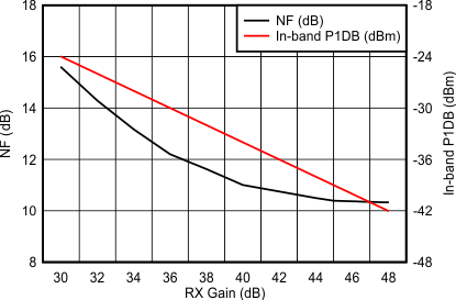
Figure 7-1 shows variations of noise figure and in-band P1dB parameters with respect to receiver gain programmed.
 Figure 7-1 Noise Figure, In-band P1dB vs Receiver
Gain