JAJSL08H september   2009  – february 2021 BQ24040 , BQ24041 , BQ24045

PRODUCTION DATA  

  1.   1
  2. 特長
  3. アプリケーション
  4. 概要
  5. Revision History
  6. Device Comparison
  7. Pin Configuration and Functions
  8. Specifications
    1. 7.1 Absolute Maximum Ratings
    2. 7.2 ESD Ratings
    3. 7.3 Recommended Operating Conditions
    4. 7.4 Thermal Information
    5. 7.5 Electrical Characteristics
    6. 7.6 Timing Requirements
    7. 7.7 Typical Operational Characteristics (Protection Circuits Waveforms)
  9. Detailed Description
    1. 8.1 Overview
    2. 8.2 Functional Block Diagram
    3. 8.3 Feature Description
      1. 8.3.1 Power-Down or Undervoltage Lockout (UVLO)
      2. 8.3.2 Power-up
      3. 8.3.3 Sleep Mode
      4. 8.3.4 New Charge Cycle
      5. 8.3.5 Overvoltage-Protection (OVP) – Continuously Monitored
      6. 8.3.6 Power Good Indication ( PG)
      7. 8.3.7 CHG Terminal Indication
    4. 8.4 Device Functional Modes
      1. 8.4.1  CHG and PG LED Pull-up Source
      2. 8.4.2  Auto Start-up (BQ24041)
      3. 8.4.3  IN-DPM (VIN-DPM or IN-DPM)
      4. 8.4.4  OUT
      5. 8.4.5  ISET
      6. 8.4.6  PRE_TERM – Pre-Charge and Termination Programmable Threshold, BQ24040/5
      7. 8.4.7  ISET2
      8. 8.4.8  TS (BQ24040/5)
      9. 8.4.9  Termination and Timer Disable Mode (TTDM) - TS Terminal High
      10. 8.4.10 Timers, BQ24040 and BQ24045 only
      11. 8.4.11 Termination
      12. 8.4.12 Battery Detect Routine
      13. 8.4.13 Refresh Threshold
      14. 8.4.14 Starting a Charge on a Full Battery
  10. Application and Implementation
    1. 9.1 Application Information
    2. 9.2 Typical Applications
      1. 9.2.1 Typical Application: BQ24040 and BQ24045
        1. 9.2.1.1 Design Requirements
        2. 9.2.1.2 Detailed Design Procedure
          1. 9.2.1.2.1 Calculations
            1. 9.2.1.2.1.1 Program the Fast Charge Current, ISET:
            2. 9.2.1.2.1.2 Program the Termination Current Threshold, ITERM:
            3. 9.2.1.2.1.3 TS Function (BQ24040)
            4. 9.2.1.2.1.4 CHG and PG
          2. 9.2.1.2.2 Selecting In and Out Terminal Capacitors
        3. 9.2.1.3 Application Curves
      2. 9.2.2 Typical Application Circuit: BQ24041, with ASI and ASO
        1. 9.2.2.1 Design Requirements
        2. 9.2.2.2 Detailed Design Procedure
        3. 9.2.2.3 Application Curves
  11. 10Power Supply Recommendations
  12. 11Layout
    1. 11.1 Layout Guidelines
    2. 11.2 Layout Example
    3. 11.3 Thermal Considerations
      1. 11.3.1 Leakage Current Effects on Battery Capacity
  13. 12Device and Documentation Support
    1. 12.1 Device Support
      1. 12.1.1 サード・パーティ製品に関する免責事項
    2. 12.2 Documentation Support
      1. 12.2.1 Related Documentation
    3. 12.3 ドキュメントの更新通知を受け取る方法
    4. 12.4 サポート・リソース
    5. 12.5 Trademarks
    6. 12.6 静電気放電に関する注意事項
    7. 12.7 用語集
  14. 13Mechanical, Packaging, and Orderable Information

パッケージ・オプション

メカニカル・データ(パッケージ|ピン)
サーマルパッド・メカニカル・データ
発注情報

New Charge Cycle

A new charge cycle is started when any of these events occur:

  • A valid power source is applied;
  • The chip is enabled/disabled using TS pin or BAT_EN;
  • Exit of termination/Timer Disable Mode (TTDM);
  • Detection of batter insertion;
  • OUT voltage drops below the VRCH threshold.

The CHG signal is active only during the first charge cycle. Exiting TTDM or the OUT voltage falling below VRCH will not activate the CHG signal if it is already in the open-drain (off) state.
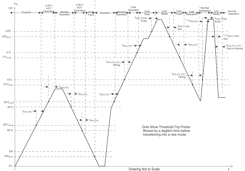
GUID-C4C5C0DA-8E03-46D1-B322-C8BA3127C502-low.gifFigure 8-2 TS Battery Temperature Bias Threshold and Deglitch Timers
GUID-189944A8-B9BD-4AE1-897F-56AAA08B0060-low.gifFigure 8-3 BQ2404x Power-Up Flow Diagram