JAJSE06A October 2017 – December 2017
PRODUCTION DATA.
- 1 特長
- 2 アプリケーション
- 3 概要
- 4 改訂履歴
- 5 概要(続き)
- 6 Device Comparison Table
- 7 Pin Configuration and Functions
- 8 Specifications
- 9 Detailed Description
- 10Application and Implementation
- 11Power Supply Recommendations
- 12Layout
- 13デバイスおよびドキュメントのサポート
- 14メカニカル、パッケージ、および注文情報
パッケージ・オプション
メカニカル・データ(パッケージ|ピン)
- RGT|16
サーマルパッド・メカニカル・データ
- RGT|16
発注情報
9.3.4.1 Input Source Connected (ADAPTER or USB)
With a source connected, the dynamic power-path management (DPPM) circuitry of the bq2407x monitors the input current continuously. For the bq24076/78, OUT is regulated to 210 mV above the voltage at BAT. When the BAT voltage falls below 3.2 V, OUT is clamped to 3.41 V. This allows for proper startup of the system load even with a discharged battery. The current into IN is shared between charging the battery and powering the system load at OUT. The bq2407x has internal selectable current limits of 100 mA (USB100) and 500 mA (USB500) for charging from USB ports, as well as a resistor-programmable input current limit.
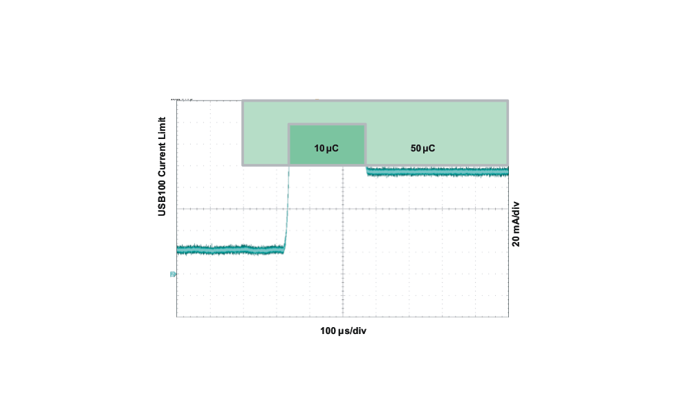
The bq2407x is USB IF compliant for the inrush current testing. The USB specification allows up to 10 μF to be hard started, which establishes 50 μC as the maximum inrush charge value when exceeding 100 mA. The input current limit for the bq2407x prevents the input current from exceeding this limit, even with system capacitances greater than 10 μF. The input capacitance to the device must be selected small enough to prevent a violation (<10 μF), as this current is not limited. Figure 14 demonstrates the start-up of the bq2407x and compares it to the USB-IF specification.
 Figure 14. USB-IF Inrush Current Test
The input current limit selection is controlled by the state of the EN1 and EN2 pins as shown in the EN1/EN2 Settings table in Pin Configuration and Functions. When using the resistor-programmable current limit, the input current limit is set by the value of the resistor connected from the ILIM pin to VSS, and is given by the equation:
The input current limit is adjustable up to 1.5 A. The valid resistor range is 1.1 kΩ to 8 kΩ.
When the IN source is connected, priority is given to the system load. The DPPM and Battery Supplement modes are used to maintain the system load. Figure 16 illustrates examples of the DPPM and supplement modes. These modes are explained in detail in the following sections.