JAJSE06A October   2017  – December 2017

PRODUCTION DATA.  

  1. 特長
  2. アプリケーション
  3. 概要
    1.     代表的なアプリケーション回路
  4. 改訂履歴
  5. 概要(続き)
  6. Device Comparison Table
  7. Pin Configuration and Functions
    1.     Pin Functions
    2. 7.1 EN1/EN2 Settings
  8. Specifications
    1. 8.1 Absolute Maximum Ratings
    2. 8.2 ESD Ratings
    3. 8.3 Recommended Operating Conditions
    4. 8.4 Thermal Information
    5. 8.5 Dissipation Ratings
    6. 8.6 Electrical Characteristics
    7. 8.7 Typical Characteristics
  9. Detailed Description
    1. 9.1 Overview
    2. 9.2 Functional Block Diagram
    3. 9.3 Feature Description
      1. 9.3.1 Undervoltage Lockout (UVLO)
      2. 9.3.2 Power On
      3. 9.3.3 Overvoltage Protection (OVP)
      4. 9.3.4 Dynamic Power-Path Management
        1. 9.3.4.1 Input Source Connected (ADAPTER or USB)
          1. 9.3.4.1.1 Input DPM Mode (VIN-DPM)
          2. 9.3.4.1.2 DPPM Mode
          3. 9.3.4.1.3 Battery Supplement Mode
        2. 9.3.4.2 Input Source Not Connected
      5. 9.3.5 Battery Charging
        1. 9.3.5.1 Charge Current Translator
        2. 9.3.5.2 Battery Detection and Recharge
        3. 9.3.5.3 Battery Disconnect (SYSOFF Input, bq24076, bq24078)
        4. 9.3.5.4 Dynamic Charge Timers (TMR Input)
        5. 9.3.5.5 Status Indicators (PGOOD, CHG)
        6. 9.3.5.6 Thermal Regulation and Thermal Shutdown
      6. 9.3.6 Battery Pack Temperature Monitoring
    4. 9.4 Device Functional Modes
      1. 9.4.1 Sleep Mode
      2. 9.4.2 Explanation of Deglitch Times and Comparator Hysteresis
  10. 10Application and Implementation
    1. 10.1 Application Information
    2. 10.2 Typical Application
      1. 10.2.1 Design Requirements
      2. 10.2.2 Detailed Design Procedure
        1. 10.2.2.1 bq2407x Charger Design Example
          1. 10.2.2.1.1 System ON/OFF (SYSOFF) (bq24076 or bq24078 only)
        2. 10.2.2.2 Calculations
          1. 10.2.2.2.1 Program the Fast Charge Current (ISET):
          2. 10.2.2.2.2 Program the Input Current Limit (ILIM)
          3. 10.2.2.2.3 Program 6.25-hour Fast-Charge Safety Timer (TMR)
        3. 10.2.2.3 TS Function
        4. 10.2.2.4 CHG and PGOOD
        5. 10.2.2.5 Selecting IN, OUT, and BAT Pin Capacitors
      3. 10.2.3 Application Curves
  11. 11Power Supply Recommendations
  12. 12Layout
    1. 12.1 Layout Guidelines
    2. 12.2 Layout Example
    3. 12.3 Thermal Considerations
  13. 13デバイスおよびドキュメントのサポート
    1. 13.1 デバイス・サポート
      1. 13.1.1 デベロッパー・ネットワークの製品に関する免責事項
    2. 13.2 関連リンク
    3. 13.3 ドキュメントの更新通知を受け取る方法
    4. 13.4 コミュニティ・リソース
    5. 13.5 商標
    6. 13.6 静電気放電に関する注意事項
    7. 13.7 Glossary
  14. 14メカニカル、パッケージ、および注文情報

パッケージ・オプション

メカニカル・データ(パッケージ|ピン)
サーマルパッド・メカニカル・データ
発注情報

Battery Supplement Mode

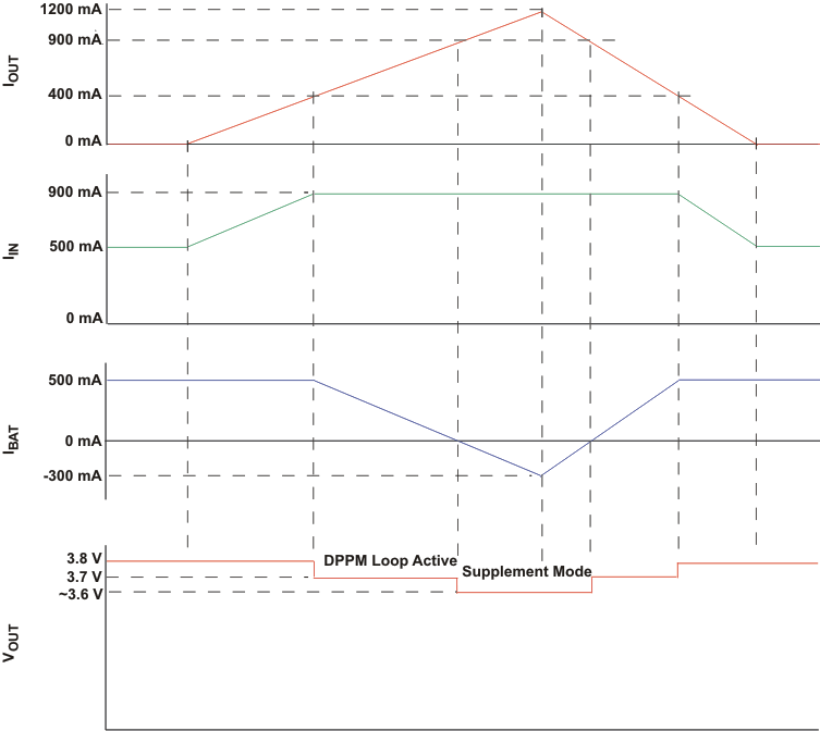
While in DPPM mode, if the charging current falls to zero and the system load current increases beyond the programmed input current limit, the voltage at OUT reduces further. When the OUT voltage drops below the VBSUP1 threshold, the battery supplements the system load. The battery stops supplementing the system load when the voltage at OUT rises above the VBSUP2 threshold.

During supplement mode, the battery supplement current is not regulated (BAT-FET is fully on), however there is a short circuit protection circuit built in. Figure 31 demonstrates supplement mode. If during battery supplement mode, the voltage at OUT drops VO(SC2) below the BAT voltage, the OUT output is turned off if the overload exists after tDGL(SC2). The short circuit recovery timer then starts counting. After tREC(SC2), OUT turns on and attempts to restart. If the short circuit remains, OUT is turned off and the counter restarts. Battery termination is disabled while in supplement mode.
bq24076 bq24078 bat_fst_chg_lus810.gifFigure 16. bq24076/78 DPPM and Battery Supplement Modes (VOREG = VBAT + 210 mV, VBAT = 3.6 V)