JAJSE21B October 2017 – November 2018
PRODUCTION DATA.
- 1 特長
- 2 アプリケーション
- 3 概要
- 4 改訂履歴
- 5 概要(続き)
- 6 Device Comparison Table
- 7 Pin Configuration and Functions
- 8 Specifications
-
9 Detailed Description
- 9.1 Overview
- 9.2 Functional Block Diagram
- 9.3 Feature Description
- 9.4 Device Functional Modes
-
10Application and Implementation
- 10.1 Application Information
- 10.2 Typical Application – bq24079QW-Q1 Charger Design Example
- 11Power Supply Recommendations
- 12Layout
- 13デバイスおよびドキュメントのサポート
- 14メカニカル、パッケージ、および注文情報
パッケージ・オプション
デバイスごとのパッケージ図は、PDF版データシートをご参照ください。
メカニカル・データ(パッケージ|ピン)
- RGT|16
サーマルパッド・メカニカル・データ
- RGT|16
発注情報
9.3.5.6 Thermal Regulation And Thermal Shutdown
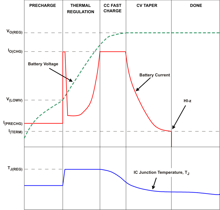
The bq24079QW-Q1 contain a thermal regulation loop that monitors the die temperature. If the temperature exceeds TJ(REG), the device automatically reduces the charging current to prevent the die temperature from increasing further. In some cases, the die temperature continues to rise despite the operation of the thermal loop, particularly under high VIN and heavy OUT system load conditions. Under these conditions, if the die temperature increases to TJ(OFF), the input FET Q1 is turned OFF. FET Q2 is turned ON to ensure that the battery still powers the load on OUT. Once the device die temperature cools by TJ(OFF-HYS), the input FET Q1 is turned on and the device returns to thermal regulation. Continuous overtemperature conditions result in a "hiccup" mode. During thermal regulation, the safety timers are slowed down proportionately to the reduction in current limit.
Note that this feature monitors the die temperature of the bq24079QW-Q1. This is not synonymous with ambient temperature. Self heating exists due to the power dissipated in the IC because of the linear nature of the battery charging algorithm and the LDO associated with OUT. A modified charge cycle with the thermal loop active is shown in Figure 24. Battery termination is disabled during thermal regulation.
 Figure 24. Charge Cycle Modified by Thermal Loop