JAJS190F March 2006 – May 2017
PRODUCTION DATA.
- 1 特長
- 2 アプリケーション
- 3 概要
- 4 改訂履歴
- 5 Pin Configuration and Functions
- 6 Specifications
-
7 Detailed Description
- 7.1 Overview
- 7.2 Functional Block Diagram
- 7.3
Feature Description
- 7.3.1 Battery Preconditioning
- 7.3.2 Battery Fast-Charge Constant Current
- 7.3.3 Charge-Current Monitor
- 7.3.4 Battery Fast-Charge Voltage Regulation
- 7.3.5 Charge Termination Detection and Recharge
- 7.3.6 Charge Status Outputs
- 7.3.7 PG Output (bq24080)
- 7.3.8 Charge-Enabled (CE) Input (bq24080)
- 7.3.9 Timer Enabled (TE) Input (bq24081)
- 7.3.10 Temperature Qualification (bq24081)
- 7.3.11 Timer Fault and Recovery
- 7.4 Device Functional Modes
- 8 Application and Implementation
- 9 Power Supply Recommendations
- 10Layout
- 11デバイスおよびドキュメントのサポート
- 12メカニカル、パッケージ、および注文情報
パッケージ・オプション
メカニカル・データ(パッケージ|ピン)
- DRC|10
サーマルパッド・メカニカル・データ
- DRC|10
発注情報
7 Detailed Description
7.1 Overview
The device supports a precision Li-Ion, Li-Pol charging system suitable for single cells. Figure 6 shows a typical charge profile, and Figure 7 shows an operational flow chart.
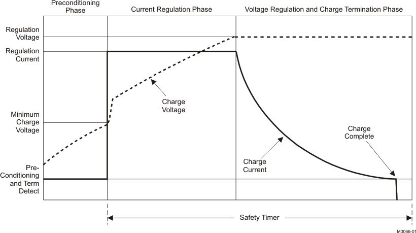 Figure 6. Typical Charging Profile
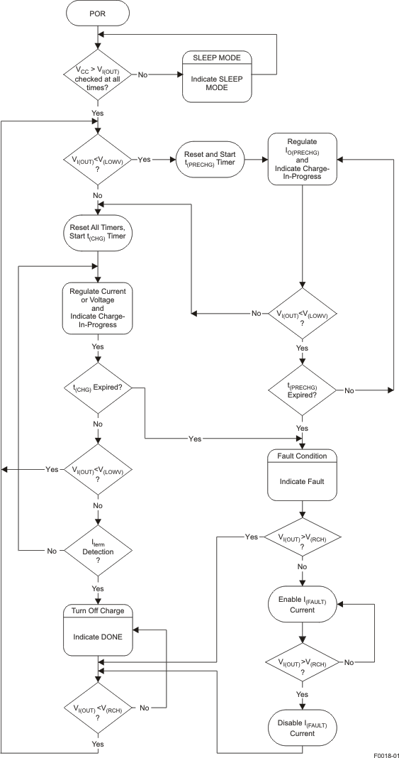 Figure 7. Operational Flow Chart
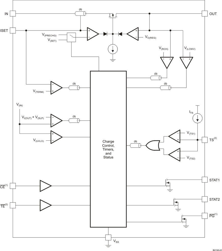
7.2 Functional Block Diagram
7.3 Feature Description
7.3.1 Battery Preconditioning
During a charge cycle, if the battery voltage is below the V(LOWV) threshold, the device applies a precharge current, IO(PRECHG), to the battery. This feature revives deeply discharged cells. Resistor RSET, connected between the ISET and VSS, determines the precharge rate. The V(PRECHG) and K(SET) parameters are specified in the Electrical Characteristics table.

The device activates a safety timer, t(PRECHG), during the conditioning phase. If the V(LOWV) threshold is not reached within the timer period, the device turns off the charger and enunciates FAULT on the STATx pins. See the Timer Fault and Recovery section for additional details.
7.3.2 Battery Fast-Charge Constant Current
The device offers on-chip current regulation with programmable set point. Resistor RSET, connected between the ISET and VSS, determines the charge rate. The V(SET) and K(SET) parameters are specified in the Electrical Characteristics table.

7.3.3 Charge-Current Monitor
When the charge function is enabled internal circuits generate a current proportional to the charge current at the ISET pin. This current, when applied to the external charge current programming resistor RISET generates an analog voltage that can be monitored by an external host to calculate the current sourced from the OUT pin.

7.3.4 Battery Fast-Charge Voltage Regulation
The voltage regulation feedback is through the OUT pin. This input is tied directly to the positive side of the battery pack. The device monitors the battery-pack voltage between the OUT and VSS pins. When the battery voltage rises to the VO(REG) threshold, the voltage regulation phase begins and the charging current begins to taper down.
As a safety backup, the device also monitors the charge time in the charge mode. If charge is not terminated within this time period, t(CHG), the charger is turned off and FAULT is set on the STATx pins. See the Timer Fault and Recovery section for additional details.
7.3.5 Charge Termination Detection and Recharge
The device monitors the charging current during the voltage regulation phase. Once the termination threshold, I(TERM), is detected, charge is terminated. The V(TERM) and K(SET) parameters are specified in the Electrical Characteristics table.

After charge termination, the device restarts the charge once the voltage on the OUT pin falls below the V(RCH) threshold. This feature keeps the battery at full capacity at all times.
The device monitors the charging current during the voltage regulation phase. Once the termination threshold, I(TERM), is detected, the charge is terminated immediately.
Resistor RSET, connected between the ISET and VSS, determines the current level at the termination threshold.
7.3.6 Charge Status Outputs
The open-drain STAT1 and STAT2 outputs indicate various charger operations as shown in Table 1. These status pins can be used to drive LEDs or communicate to the host processor. Note that OFF indicates the open-drain transistor is turned off.
Table 1. Status Pin Summary
| CHANGE STATE | STAT1 | STAT2 |
|---|---|---|
| Precharge in progress | ON | ON |
| Fast charge in progress | ON | OFF |
| Charge done | OFF | ON |
| Charge suspend (temperature) | OFF | OFF |
| Timer fault | ||
| Sleep mode |
7.3.7 PG Output (bq24080)
The open-drain power-good (PG) output pulls low when a valid input voltage is present. This output is turned off (high-impedance) in sleep mode. The PG pin can be used to drive an LED or communicate to the host processor.
7.3.8 Charge-Enabled (CE) Input (bq24080)
The CE digital input is used to disable or enable the charge process. A low-level signal on this pin enables the charge and a high-level signal disables the charge and places the device in a low-power mode. A high-to-low transition on this pin also resets all timers and timer fault conditions.
7.3.9 Timer Enabled (TE) Input (bq24081)
The TE digital input is used to disable or enable the fast-charge timer. A low-level signal on this pin enables the fast-charge timer, and a high-level signal disables this feature.
7.3.10 Temperature Qualification (bq24081)
The bq24081 continuously monitors battery temperature by measuring the voltage between the TS and VSS pins. An internal current source provides the bias for common 10-kΩ negative-temperature-coefficient thermistors (NTC) (see the functional block diagram). The device compares the voltage on the TS pin with the internal V(TS1) and V(TS2) thresholds to determine if charging is allowed. If a temperature outside the V(TS1) and V(TS2) thresholds is detected, the device immediately suspends the charge by turning off the power FET and holding the timer value (i.e., timers are not reset). Charge is resumed when the temperature returns within the normal range.
The allowed temperature range with a 103AT-type thermistor is 0°C to 45°C. However, the user may modify these thresholds by adding external resistors (see Figure 8 and Figure 9
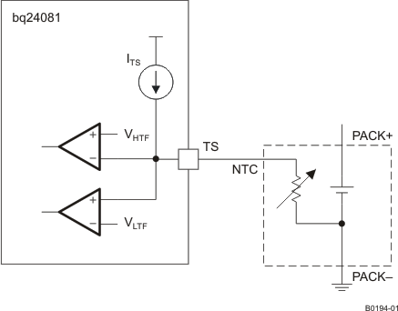 Figure 8. Default Temperature Thresholds
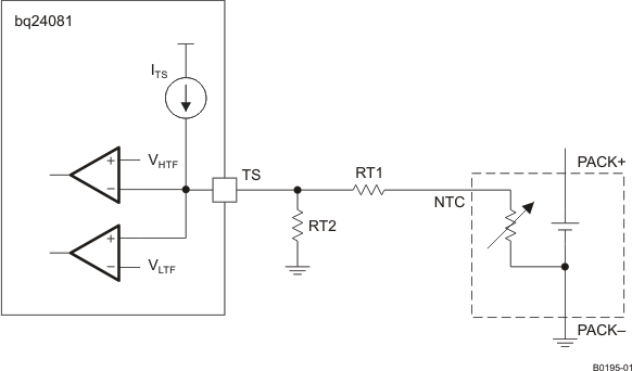 Figure 9. Temperature Thresholds Modified by External Resistors
7.3.11 Timer Fault and Recovery
As shown in Figure 7, the device provides a recovery method to deal with timer fault conditions. The following summarizes this method:
7.3.11.1 Condition Number 1
OUT pin voltage is above the recharge threshold (V(RCH)), and a timeout fault occurs.
Recovery method: the device waits for the OUT pin voltage to fall below the recharge threshold. This could happen as a result of a load on the battery, self-discharge, or battery removal. Once the OUT pin voltage falls below the recharge threshold, the device clears the fault and starts a new charge cycle. A POR, TE, or CE toggle also clears the fault.
7.3.11.2 Condition Number 2
OUT pin voltage is below the recharge threshold (V(RCH)), and a timeout fault occurs
Recovery method: Under this scenario, the device applies the I(FAULT) current. This small current is used to detect a battery removal condition and remains on as long as the battery voltage stays below the recharge threshold. If the OUT pin voltage goes above the recharge threshold, then the device disables the I(FAULT) current and executes the recovery method described for condition number 1. Once the OUT pin voltage falls below the recharge threshold, the bq24080 clears the fault and starts a new charge cycle. A POR, TE, or CE toggle also clears the fault.
7.4 Device Functional Modes
7.4.1 Sleep Mode
The device enters the low-power sleep mode if the input power (IN) is removed from the circuit. This feature prevents draining the battery during the absence of input supply.