JAJS190F March 2006 – May 2017
PRODUCTION DATA.
- 1 特長
- 2 アプリケーション
- 3 概要
- 4 改訂履歴
- 5 Pin Configuration and Functions
- 6 Specifications
-
7 Detailed Description
- 7.1 Overview
- 7.2 Functional Block Diagram
- 7.3
Feature Description
- 7.3.1 Battery Preconditioning
- 7.3.2 Battery Fast-Charge Constant Current
- 7.3.3 Charge-Current Monitor
- 7.3.4 Battery Fast-Charge Voltage Regulation
- 7.3.5 Charge Termination Detection and Recharge
- 7.3.6 Charge Status Outputs
- 7.3.7 PG Output (bq24080)
- 7.3.8 Charge-Enabled (CE) Input (bq24080)
- 7.3.9 Timer Enabled (TE) Input (bq24081)
- 7.3.10 Temperature Qualification (bq24081)
- 7.3.11 Timer Fault and Recovery
- 7.4 Device Functional Modes
- 8 Application and Implementation
- 9 Power Supply Recommendations
- 10Layout
- 11デバイスおよびドキュメントのサポート
- 12メカニカル、パッケージ、および注文情報
パッケージ・オプション
メカニカル・データ(パッケージ|ピン)
- DRC|10
サーマルパッド・メカニカル・データ
- DRC|10
発注情報
8 Application and Implementation
NOTE
Information in the following applications sections is not part of the TI component specification, and TI does not warrant its accuracy or completeness. TI’s customers are responsible for determining suitability of components for their purposes. Customers should validate and test their design implementation to confirm system functionality.
8.1 Application Information
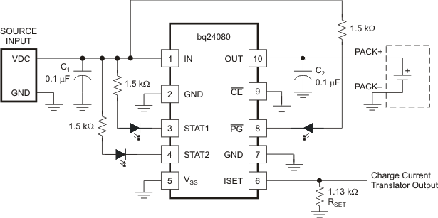
The bq24080 and bq24081 are highly integrated and flexible Li-Ion linear charge devices targeted at space-limited charger applications. They offer an integrated power FET and current sensor, high accuracy current and voltage regulation, charge status, and charge termination, in a single monolithic device. An external resistor sets the magnitude of the charge current.
8.2 Typical Application
 Figure 10. Typical Application Circuit
8.2.1 Design Requirements
For this design example, use the parameters shown in Table 2.
Table 2. Design Parameters
| PARAMETER | VALUE |
|---|---|
| Supply voltage | 5 V |
| Fast-charge current | ≈ 750 mA |
| Battery-Temperature sense (bq24081-Q1) | –2°C to 44.5°C (default setting) |
8.2.2 Detailed Design Procedure
8.2.2.1 Calculations
Program the charge current for 750 mA:
From Electrical Characteristics table, V(SET) = 2.5 V.
From Electrical Characteristics table, K(SET) = 322.
Selecting the closest standard value, use a 1.07-kΩ resistor connected between ISET (pin 6) and ground.
8.2.2.2 Battery Temperature Sense (bq24081)
Use a Semitec 103AT-4 NTC thermistor connected between TS (pin 9) and ground.
Look up the corresponding temperature value in the manufacturer's resistance-temperature table for the thermistor selected. For a 103AT-4 Semitec thermistor:
5 kΩ = 44.5°C
25 kΩ = 2°C
8.2.2.3 STAT Pins (All Devices) and PG Pin (bq24080)
Status pins Monitored by Processor:
Select a pullup resistor that can source more than the input bias (leakage) current of both the processor and status pins and still provide a logic high.
Connect a 100-kΩ pullup between each status pin and the VCC of the processor. Connect each status pin to a μP monitor pin.
Status viewed by LED:
Select an LED with a current rating less than 10 mA and select a resistor to place in series with the LED to limit the current to the desired current value (brightness).
Place an LED and resistor in series between the input and each status pin.
8.2.2.4 Selecting Input and Output Capacitors
In most applications, all that is needed is a high-frequency decoupling capacitor on the input power pin. A 0.1-μF ceramic capacitor, placed in close proximity to the IN pin and GND pad works well. In some applications, it may be necessary to protect against a hot plug input voltage overshoot. This is done in three ways:
- The best way is to add an input zener, 6.2 V, between the IN pin and VSS.
- A low-power zener is adequate for the single event transient. Increasing the input capacitance lowers the characteristic impedance which makes the input resistance move effective at damping the overshoot, but risks damaging the input contacts by the high inrush current.
- Placing a resistor in series with the input dampens the overshoot, but causes excess power dissipation.
The device only requires a small capacitor for loop stability. A 0.1-μF ceramic capacitor placed between the OUT and GND pad is typically sufficient.
8.2.3 Application Curves

(CE = High-to-Low)

| No battery – In termination deglitch prior to STAT1 going high. VOUT (VBAT) cycling between charge and done prior to screen capture | ||
| Stat1 goes high – In done state | ||
| 2-V battery is inserted during the charge done state. | ||
| Charging is initiated – STAT1 goes low and charge current is applied. | ||
| Battery is removed – VOUT goes into regulation, IOUT goes to zero, and termination deglitch timer starts running (same as state 1). | ||
| Deglitch timer expires – charge done is declared. |