SLUS688H March 2006 – November 2015
PRODUCTION DATA.
- 1 Features
- 2 Applications
- 3 Description
- 4 Revision History
- 5 Device Options
- 6 Pin Configuration and Functions
- 7 Specifications
-
8 Detailed Description
- 8.1 Overview
- 8.2 Functional Block Diagram
- 8.3
Feature Description
- 8.3.1 PWM Controller
- 8.3.2 Temperature Qualification
- 8.3.3 Battery Preconditioning (Precharge)
- 8.3.4 Battery Charge Current
- 8.3.5 Battery Voltage Regulation
- 8.3.6 Charge Termination And Recharge
- 8.3.7 Sleep Mode
- 8.3.8 Charge Status Outputs
- 8.3.9 PG Output
- 8.3.10 CE Input (Charge Enable)
- 8.3.11 Timer Fault Recovery
- 8.3.12 Output Overvoltage Protection (Applies to All Versions)
- 8.3.13 Battery Detection
- 8.3.14 Current Sense Amplifier
- 8.4 Device Functional Modes
- 9 Application and Implementation
- 10Power Supply Recommendations
- 11Layout
- 12Device and Documentation Support
- 13Mechanical, Packaging, and Orderable Information
パッケージ・オプション
メカニカル・データ(パッケージ|ピン)
- RHL|20
サーマルパッド・メカニカル・データ
- RHL|20
発注情報
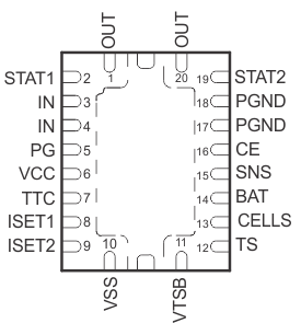
6 Pin Configuration and Functions
RHL Package
20-Pin VQFN
Top View

Pin Functions
| PIN | I/O | DESCRIPTION | |||
|---|---|---|---|---|---|
| NAME | bq24120 | bq24123 | bq24125 | ||
| BAT | 14 | 14 | 14 | I | Battery voltage sense input. Bypass it with a capacitor to VSS if there are long inductive leads to battery. |
| CE | 16 | 16 | 16 | I | Charger enable input. This active low input, if set high, suspends charge and places the device in the low-power sleep mode. Do not pull up this input to VTSB. |
| CELLS | 13 | I | Available on parts with selectable output voltage. Ground or float for single-cell operation (4.2 V). For two-cell operation (8.4 V) pull up this pin with a resistor to VIN. | ||
| FB | 13 | I | Output voltage analog feedback adjustment. Connect the output of a resistive voltage divider powered from the battery terminals to this node to adjust the output battery voltage regulation. | ||
| IN | 3, 4 | 3, 4 | 3, 4 | I | Charger input voltage. Bypass it with a 10μF capacitor from IN to PGND. |
| ISET1 | 8 | 8 | 8 | I/O | Charger current set point 1 (fast charge). Use a resistor to ground to set this value. |
| ISET2 | 9 | 9 | 9 | I/O | Charge current set point 2 (precharge and termination), set by a resistor connected to ground. |
| N/C | 13 | – | No connection. This pin must be left floating in the application. | ||
| OUT | 1 | 1 | 1 | O | Charge current output inductor connection. Connect a zener TVS diode between OUT pin and PGND to clamp the voltage spike to protect the power MOSFETs during abnormal conditions. |
| 20 | 20 | 20 | O | ||
| PG | 5 | 5 | 5 | O | Power-good status output (open drain). The transistor turns on when a valid VCC is detected. It is turned off in the sleep mode. PG can be used to drive a LED or communicate with a host processor. |
| PGND | 17,18 | 17,18 | 17,18 | Power ground input | |
| SNS | 15 | 15 | 15 | I | Charge current-sense input. Battery current is sensed via the voltage drop developed on this pin by an external sense resistor in series with the battery pack. A 0.1μF capacitor to VSS is required. |
| STAT1 | 2 | 2 | 2 | O | Charge status 1 (open-drain output). When the transistor turns on indicates charge in process. When it is off and with the condition of STAT2 indicates various charger conditions (See Table 1) |
| STAT2 | 19 | 19 | 19 | O | Charge status 2 (open-drain output). When the transistor turns on indicates charge is done. When it is off and with the condition of STAT1 indicates various charger conditions (See Table 1) |
| TS | 12 | 12 | 12 | I | Temperature sense input. This input monitors its voltage against an internal threshold to determine if charging is allowed. Use an NTC thermistor and a voltage divider powered from VTSB to develop this voltage. (See Figure 9) |
| TTC | 7 | 7 | 7 | I | Timer and termination control. Connect a capacitor from this node to VSS to set the bqSWITCHER timer. When this input is low, the timer and termination detection are disabled. |
| VCC | 6 | 6 | 6 | I | Analog device input. A 0.1μF capacitor to VSS is required. |
| VSS | 10 | 10 | 10 | Analog ground input | |
| VTSB | 11 | 11 | 11 | O | TS internal bias regulator voltage. Connect capacitor (with a value between a 0.1μF and 1μF) between this output and VSS. |
| Exposed Thermal Pad |
Pad | Pad | Pad | There is an internal electrical connection between the exposed thermal pad and VSS. The exposed thermal pad must be connected to the same potential as the VSS pin on the printed circuit board. The power pad can be used as a star ground connection between VSS and PGND. A common ground plane may be used. VSS pin must be connected to ground at all times. | |