JAJSEC4E September   2012  – January 2018

PRODUCTION DATA.  

  1. 特長
  2. アプリケーション
  3. 概要
    1.     代表的なアプリケーション回路
  4. 改訂履歴
  5. 概要(続き)
  6. Device Comparisons
  7. Pin Configuration and Functions
    1.     Pin Functions
  8. Specifications
    1. 8.1 Absolute Maximum Ratings
    2. 8.2 ESD Ratings
    3. 8.3 Recommended Operating Conditions
    4. 8.4 Thermal Information
    5. 8.5 Electrical Characteristics
    6. 8.6 Timing Requirements
    7. 8.7 Typical Characteristics
  9. Detailed Description
    1. 9.1 Overview
    2. 9.2 Functional Block Diagrams
    3. 9.3 Operational Flow Chart
    4. 9.4 Feature Description
      1. 9.4.1 Input Voltage Protection
        1. 9.4.1.1 Input Overvoltage Protection
        2. 9.4.1.2 Bad Adaptor Detection/Rejection
        3. 9.4.1.3 Sleep Mode
        4. 9.4.1.4 Input Voltage Based DPM (Special Charger Voltage Threshold)
      2. 9.4.2 Battery Protection
        1. 9.4.2.1 Output Overvoltage Protection
        2. 9.4.2.2 Battery Detection at Power Up in DEFAULT Mode
        3. 9.4.2.3 Battery Short Protection
        4. 9.4.2.4 Battery Detection in Host Mode
      3. 9.4.3 DEFAULT Mode
      4. 9.4.4 USB Friendly Power Up
      5. 9.4.5 Input Current Limiting At Power Up
    5. 9.5 Device Functional Modes
      1. 9.5.1 Charge Mode Operation
        1. 9.5.1.1 Charge Profile
      2. 9.5.2 PWM Controller in Charge Mode
      3. 9.5.3 Battery Charging Process
      4. 9.5.4 Thermal Regulation and Protection
      5. 9.5.5 Charge Status Output, STAT Pin
      6. 9.5.6 Control Bits in Charge Mode
        1. 9.5.6.1 CE Bit (Charge Mode)
        2. 9.5.6.2 RESET Bit
        3. 9.5.6.3 OPA_Mode Bit
      7. 9.5.7 Control Pins in Charge Mode
        1. 9.5.7.1 CD Pin (Charge Disable)
      8. 9.5.8 BOOST Mode Operation
        1. 9.5.8.1 PWM Controller in Boost Mode
        2. 9.5.8.2 Boost Start Up
        3. 9.5.8.3 PFM Mode at Light Load
        4. 9.5.8.4 Protection in Boost Mode
          1. 9.5.8.4.1 Output Overvoltage Protection
          2. 9.5.8.4.2 Output Overload Protection
          3. 9.5.8.4.3 Battery Overvoltage Protection
        5. 9.5.8.5 STAT Pin in Boost Mode
      9. 9.5.9 High Impedance (Hi-Z) Mode
    6. 9.6 Programming
      1. 9.6.1 Serial Interface Description
        1. 9.6.1.1 F/S Mode Protocol
        2. 9.6.1.2 H/S Mode Protocol
        3. 9.6.1.3 I2C Update Sequence
        4. 9.6.1.4 Slave Address Byte
        5. 9.6.1.5 Register Address Byte
    7. 9.7 Register Description
  10. 10Application and Implementation
    1. 10.1 Application Information
      1. 10.1.1 Typical Application
        1. 10.1.1.1 Design Requirements
        2. 10.1.1.2 Detailed Design Procedure
      2. 10.1.2 Charge Current Sensing Resistor Selection Guidelines
      3. 10.1.3 Output Inductor and Capacitance Selection Guidelines
    2. 10.2 Typical Performance Curves
  11. 11Power Supply Recommendations
    1. 11.1 System Load After Sensing Resistor
      1. 11.1.1 The Advantages:
      2. 11.1.2 Design Requirements and Potential Issues:
  12. 12Layout
    1. 12.1 Layout Guidelines
    2. 12.2 Layout Example
  13. 13デバイスおよびドキュメントのサポート
    1. 13.1 ドキュメントのサポート
      1. 13.1.1 デベロッパー・ネットワークの製品に関する免責事項
    2. 13.2 ドキュメントの更新通知を受け取る方法
    3. 13.3 コミュニティ・リソース
    4. 13.4 商標
    5. 13.5 静電気放電に関する注意事項
    6. 13.6 Glossary
  14. 14メカニカル、パッケージ、および注文情報
    1. 14.1 パッケージ概要
      1. 14.1.1 チップ・スケール・パッケージの寸法

パッケージ・オプション

メカニカル・データ(パッケージ|ピン)
サーマルパッド・メカニカル・データ
発注情報

I2C Update Sequence

The IC requires a start condition, a valid I2C address, a register address byte, and a data byte for a single update. After the receipt of each byte, the IC acknowledges by pulling the SDA line low during the high period of a single clock pulse. A valid I2C address selects the IC. The IC performs an update on the falling edge of the acknowledge signal that follows the LSB byte.

For the first update, the IC requires a start condition, a valid I2C address, a register address byte, a data byte. For all consecutive updates, The IC needs a register address byte, and a data byte. Once a stop condition is received, the IC releases the I2C bus, and awaits a new start conditions.
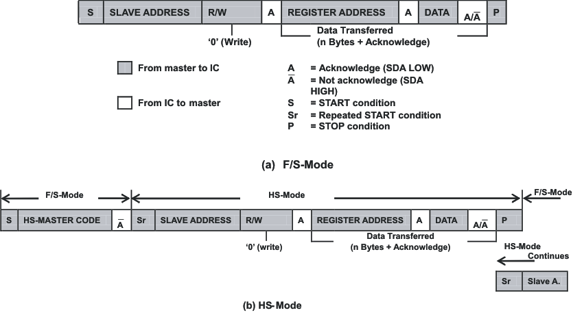
bq24157 register_lusa27.gifFigure 22. Data Transfer Format in F/S Mode and H/S Mode