SLUSAF2C February 2011 – April 2015
PRODUCTION DATA.
- 1 Features
- 2 Applications
- 3 Description
- 4 Revision History
- 5 Description (Continued)
- 6 Device Comparison Table
- 7 Pin Configuration and Functions
- 8 Specifications
-
9 Detailed Description
- 9.1 Overview
- 9.2 Functional Block Diagram
- 9.3
Feature Description
- 9.3.1 Battery Voltage Regulation
- 9.3.2 Battery Current Regulation
- 9.3.3 Battery Precharge Current Regulation
- 9.3.4 Input Current Regulation
- 9.3.5 Charge Termination, Recharge, and Safety Timers
- 9.3.6 Power Up
- 9.3.7 Input Undervoltage Lockout (UVLO)
- 9.3.8 Input Overvoltage/Undervoltage Protection
- 9.3.9 Enable and Disable Charging
- 9.3.10 System Power Selector
- 9.3.11 Converter Operation
- 9.3.12 Automatic Internal Soft-Start Charger Current
- 9.3.13 Charge Overcurrent Protection
- 9.3.14 Charge Undercurrent Protection
- 9.3.15 Battery Detection
- 9.3.16 Battery Short Protection
- 9.3.17 Battery Overvoltage Protection
- 9.3.18 Temperature Qualification and JEITA Guideline
- 9.3.19 MOSFET Short Circuit and Inductor Short Circuit Protection
- 9.3.20 Thermal Regulation and Shutdown Protection
- 9.3.21 Timer Fault Recovery
- 9.3.22 Inductor, Capacitor, and Sense Resistor Selection Guidelines
- 9.3.23 Charge Status Outputs
- 9.4 Device Functional Modes
- 10Application and Implementation
- 11Power Supply Recommendations
- 12Layout
- 13Device and Documentation Support
- 14Mechanical, Packaging, and Orderable Information
1 Features
- JEITA-Compatible Battery Temperature Sensing
- 1.6-MHz Synchronous Switched-Mode Charger With 4-A Integrated N-MOSFETs
- Up to 94% Efficiency
- 30-V Input Rating With Adjustable Overvoltage Protection
- 4.5-V to 17-V Input Operating Voltage
-
Battery Charge Voltage
- Adjustable Charge Voltage up to 3-Series Cells
- High Integration
- Automatic Power Path Selector Between Adapter and Battery
- Dynamic Power Management
- Integrated 20-V Switching MOSFETs
- Integrated Bootstrap Diode
- Internal Loop Compensation
- Internal Digital Soft Start
- Safety
- Thermal Regulation Loop Throttles Back Current to Limit TJ = 120°C
- Thermal Shutdown
- Battery Thermistor Sense Hot/Cold Charge Suspend and Battery Detect
- Input Overvoltage Protection With Programmable Threshold
- Cycle-by-Cycle Current Limit
- Accuracy
- ±0.5% Charge Voltage Regulation
- ±4% Charge Current Regulation
- ±4% Input Current Regulation
- Less Than 15-μA Battery Current With Adapter Removed
- Less Than 1.5-mA Input Current With Adapter Present and Charge Disabled
- Small QFN Package
2 Applications
- Tablet PCs
- Netbooks and Ultra-Mobile Computers
- Portable Data Capture Terminals
- Portable Printers
- Medical Diagnostics Equipment
- Battery Bay Chargers
- Battery Backup Systems
3 Description
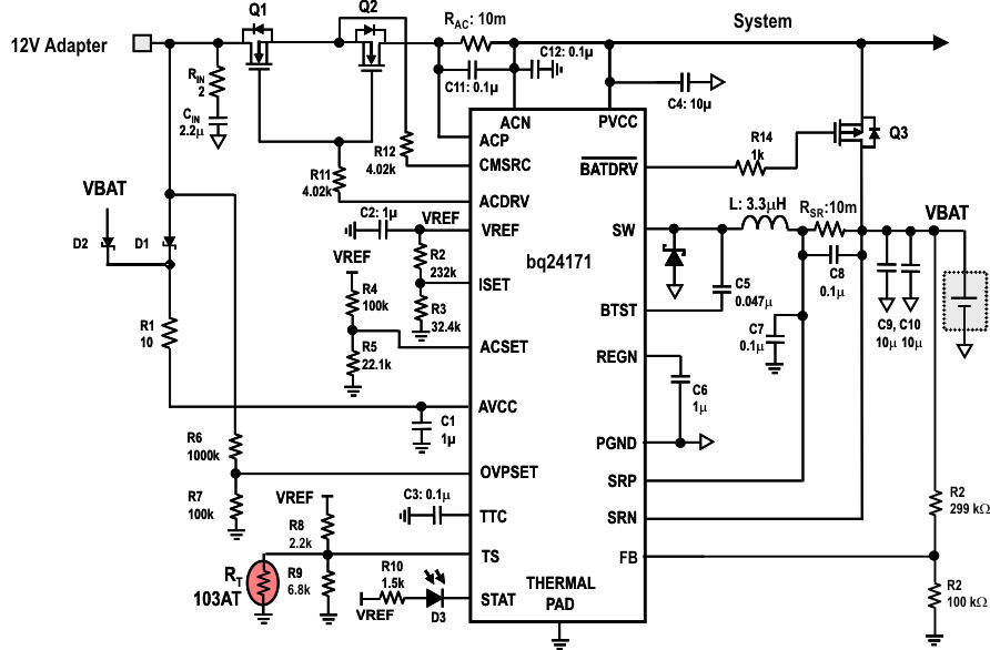
The bq24171 device is highly integrated stand-alone Li-ion and Li-polymer switched-mode battery charger with two integrated N-channel power MOSFETs. The device offers a constant-frequency synchronous PWM controller with high-accuracy regulation of input current, charge current, and voltage. The bq24171 closely monitors the battery pack temperature and allows charge only in a JEITA profile-compatible window with a lower charge rate at a low temperature and a lower charge voltage at a high temperature. The bq24171 device charges the battery in three phases: preconditioning, constant current, and constant voltage. The bq24171 charges up to 3-series cells with an adjustable cell voltage.
Device Information(1)
| PART NUMBER | PACKAGE | BODY SIZE (NOM) |
|---|---|---|
| bq24171 | VQFN (24) | 5.50 mm × 3.50 mm |
- For all available packages, see the orderable addendum at the end of the data sheet.
Typical Application Schematic

4 Revision History
Changes from B Revision (October 2013) to C Revision
- Added ESD Ratings table, Feature Description section, Device Functional Modes, Application and Implementation section, Power Supply Recommendations section, Layout section, Device and Documentation Support section, and Mechanical, Packaging, and Orderable Information sectionGo
Changes from A Revision (April 2011) to B Revision
- Changed publication to Rev B, October 2013Go
- Changed figure reference pointer from "Figure 22" to "Figure 23" in INPUT ADFET AND RBDET SELECTION decscription.Go
- Changed resistor name in Figure 21 from "Rsns" to "Rac".Go
- Changed Figure 23 diode D1 symbol to a more distinct image to show it is a Schottky diode.Go
Changes from * Revision (February 2011) to A Revision
- Changed publication to Rev A, May 2011Go
- Changed the 4th FEATURES bullet from "4.5V to 17V Input Operating Voltage" to "30V Input Rating with Adjustable Over-Voltage Protection" and sub-bullet "4.5V to 17V Input Operating Voltage"Go
- Added esds note to top of second page; added "DESCRIPTION (Continued)" title on second page; and new paragraph on page 2 (beginning "The bq24171 charges battery from DC source as high as 17V.")Go
- Changed ABS MAX table first-row descriptors from "PVCC, AVCC, ACN, CMSRC, STAT" to "AVCC, ACP, ACN, ACDRV, CMSRC, STAT" and second-row descriptor from "ACDRV, BTST" to "PVCC"; changed PVCC max voltage from 30V to 20V Go
- Changed hyperlink to point to Design Tool sluc244aGo
- Added new paragraph under INPUT FILTER DESIGN section (beginning..."If the input is 5V....")Go
- Added connection between CMSRC and ACP in Figure 2 Typical Application schematic.Go