SLUSB97A October 2012 – December 2014
PRODUCTION DATA.
- 1 Features
- 2 Applications
- 3 Description
- 4 Revision History
- 5 Description (Continued)
- 6 Pin Configuration and Functions
- 7 Specifications
-
8 Detailed Description
- 8.1 Overview
- 8.2 Functional Block Diagram
- 8.3
Feature Description
- 8.3.1 Device Power Up
- 8.3.2 Power Path Management
- 8.3.3 Battery Charging Management
- 8.3.4 Status Outputs (STAT and INT)
- 8.3.5 Protections
- 8.3.6 Serial Interface
- 8.4 Device Functional Modes
- 8.5
Register Map
- 8.5.1
I2C Registers
- 8.5.1.1 Input Source Control Register REG00 (reset = 00110000, or 30)
- 8.5.1.2 Power-On Configuration Register REG01 (reset = 00011011, or 1B)
- 8.5.1.3 Charge Current Control Register REG02 (reset = 01100000, or 60)
- 8.5.1.4 Pre-Charge/Termination Current Control Register REG03 (reset = 00010001, or 11)
- 8.5.1.5 Charge Voltage Control Register REG04 (reset = 10110010, or B2)
- 8.5.1.6 Charge Termination/Timer Control Register REG05 (reset = 10011010, or 9A)
- 8.5.1.7 Thermal Regulation Control Register REG06 (reset = 00000011, or 03)
- 8.5.1.8 Misc Operation Control Register REG07 (reset = 01001011, or 4B)
- 8.5.1.9 System Status Register REG08
- 8.5.1.10 Fault Register REG09
- 8.5.1.11 Vender / Part / Revision Status Register REG0A (reset = 00100011, or 23)
- 8.5.1
I2C Registers
- 9 Application and Implementation
- 10Power Supply Recommendations
- 11Layout
- 12Device and Documentation Support
- 13Mechanical, Packaging, and Orderable Information
パッケージ・オプション
メカニカル・データ(パッケージ|ピン)
- RGE|24
サーマルパッド・メカニカル・データ
- RGE|24
発注情報
9 Application and Implementation
NOTE
Information in the following applications sections is not part of the TI component specification, and TI does not warrant its accuracy or completeness. TI’s customers are responsible for determining suitability of components for their purposes. Customers should validate and test their design implementation to confirm system functionality.
9.1 Application Information
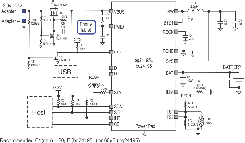
A typical application consists of the device configured as an I2C controlled power path management device and a single cell Li-Ion battery charger for single cell Li-Ion and Li-polymer batteries used in a wide range of tablets and other portable devices. It integrates an input reverse-blocking FET (RBFET, Q1), high-side switching FET (HSFET, Q2), low-side switching FET (LSFET, Q3), and BATFET (Q4) between the system and battery. The device also integrates a bootstrap diode for the high-side gate drive.
9.2 Typical Application

9.2.1 Design Requirements
Table 18. Design Requirements
| DESIGN PARAMETER | EXAMPLE VALUE |
|---|---|
| Input voltage | 3.9 V to 17 V |
| Input current limit | 1.5 A |
| Fast charge current | 2048 mA |
| Boost mode output current | 2.5 A (bq24195L) or 4.5 A (bq24195) |
9.2.2 Detailed Design Procedure
9.2.2.1 Inductor Selection
The bq24195L, bq24195 has 1.5-MHz switching frequency to allow the use of small inductor and capacitor values. The Inductor saturation current should be higher than the charging current (ICHG) plus half the ripple current (IRIPPLE):

The inductor ripple current depends on input voltage (VBUS), duty cycle (D = VBAT/VVBUS), switching frequency (fs) and inductance (L):

The maximum inductor ripple current happens with D = 0.5 or close to 0.5. Usually inductor ripple is designed in the range of (20 to 40%) maximum charging current as a trade-off between inductor size and efficiency for a practical design. Typical inductor value is 2.2 µH.
9.2.2.2 Input Capacitor
Input capacitor should have enough ripple current rating to absorb input switching ripple current. The worst case RMS ripple current is half of the charging current when duty cycle is 0.5. If the converter does not operate at 50% duty cycle, then the worst case capacitor RMS current ICIN occurs where the duty cycle is closest to 50% and can be estimated by the following equation:

For best performance, VBUS should be decouple to PGND with 1-μF capacitance. The remaining input capacitor should be place on PMID.
Low ESR ceramic capacitor such as X7R or X5R is preferred for input decoupling capacitor and should be placed to the drain of the high side MOSFET and source of the low side MOSFET as close as possible. Voltage rating of the capacitor must be higher than normal input voltage level. 25-V rating or higher capacitor is preferred for 15-V input voltage.
9.2.2.3 Output Capacitor
Output capacitor also should have enough ripple current rating to absorb output switching ripple current. The output capacitor RMS current ICOUT is given:

The output capacitor voltage ripple can be calculated as follows:

At certain input/output voltage and switching frequency, the voltage ripple can be reduced by increasing the output filter LC.
The charger device has internal loop compensator. To get good loop stability, the resonant frequency of the output inductor and output capacitor should be designed between 15 kHz and 25 kHz. With 2.2-µH inductor, the typical output capacitor value is 20 µF. The preferred ceramic capacitor is 6 V or higher rating, X7R or X5R.
9.2.3 Application Performance Plots

| VBAT 3.2 V | ||||

| VBUS 12 V | ||||

| VBUS 12 V, VBAT 3.8 V, ICHG 3 A | ||

| VBAT 3.8 V, ILOAD 1 A | ||

| VBUS 5 V | ||||

| VBUS 5 V, IIN 3 A, Charge Disable | ||

| VBUS 9 V, No Battery, ISYS 10 mA, Charge Disable | ||

| VBAT 3.8 V | ||||