bq24196 I2C Controlled 2.5-A Single Cell USB/Adapter Charger with Narrow VDC Power Path Management and USB OTG
1 Features
- High Efficiency 2.5-A Switch Mode Charger
- 92% Charge Efficiency at 2 A
- Highest Battery Discharge Efficiency with 12-mΩ Battery Discharge MOSFET up to 9-A Discharge Current
- Single Input USB-compliant/Adapter Charger
- Input Voltage and Current Limit Supports USB2.0 and USB3.0
- Input Current Limit: 100 mA, 150 mA, 500 mA, 900 mA, 1.2 A, 1.5 A, 2 A and 3 A
- 3.9-V to 17-V Input Operating Voltage Range
- Support All Kinds of Adapter with Input Voltage DPM Regulation
- USB OTG 5 V at 1.3-A Synchronous Boost Converter Operation
- 93% 5-V Boost Efficiency at 1 A
- Narrow VDC (NVDC) Power Path Management
- Instant-on Works with No Battery or Deeply Discharged Battery
- Ideal Diode Operation in Battery Supplement Mode
- 1.5-MHz Switching Frequency for Low Profile Inductor
- Autonomous Battery Charging with or without Host Management
- Battery Charge Enable
- Battery Charge Preconditioning
- Charge Termination and Recharge
- High Accuracy (0°C to 125°C)
- ±0.5% Charge Voltage Regulation
- ±7% Charge Current Regulation
- ±7.5% Input Current Regulation
- ±2% Output Regulation in Boost Mode
- High Integration
- Power Path Management
- Synchronous Switching MOSFETs
- Integrated Current Sensing
- Bootstrap Diode
- Internal Loop Compensation
- Safety
- Battery Temperature Sensing and Charging Safety Timer
- Thermal Regulation and Thermal Shutdown
- Input System Over-Voltage Protection
- MOSFET Over-Current Protection
- Charge Status Outputs for LED or Host Processor
- Low Battery Leakage Current and Support Shipping Mode
- 4.00 mm x 4.00 mm VQFN-24 Package
2 Applications
- Tablet PC and Smart Phone
- Portable Audio Speaker
- Portable Media Players
- Internet Devices
3 Description
The bq24196 is highly-integrated switch-mode battery charge management and system power path management devices for single cell Li-Ion and Li-polymer battery in a wide range of tablet and other portable devices.
Device Information(1)
| PART NUMBER | PACKAGE | BODY SIZE (NOM) |
|---|---|---|
| bq24196 | VQFN (24) | 4.00 mm x 4.00 mm |
- For all available packages, see the orderable addendum at the end of the datasheet.
4 Revision History
Changes from * Revision (October 2012) to A Revision
- Added Handling Rating table, Feature Description section, Device Functional Modes, Application and Implementation section, Power Supply Recommendations section, Layout section, Device and Documentation Support section, and Mechanical, Packaging, and Orderable Information section. Go
- Changed BOOT to BTST in bq24196 with PSEL from PHY, charging from SDP/DCP, and Two Thermistor ConnectionsGo
- Changed VSLEEPZ, VBAT_DPL_HY, VBATGD , ICHG_20pct, VSHORT, IADPT_DPM, KILIM, VBTST_REFRESH in Electrical CharacteristicsGo
- Added –40°C to 85° to IBAT Test ConditionGo
- Added REG00[6:3] = 0110 (4.36 V) or 1011 (4.76 V) to VINDPM_REG_ACC Test ConditionsGo
- Added a MIN value of 435 to KILIMGo
- Deleted TJunction_REG MIN and MAXGo
- Changed VOTG_ILIM to IOTG_ILIM and VOTG_HSZCP to IOTG_HSZCPGo
- Deleted VREGN, VVBUS = 5 V, IREGN = 20 mA MAX valueGo
- Changed Functional Block DiagramGo
- Changed REG09[5:4] to REG08[5:4] in Charging Termination sectionGo
- Changed Charging Safety Timer descriptionGo
- Changed Host Mode and Default Mode descriptionGo
- Changed Charge Current Control Register REG02 Bit 0 description and noteGo
- Changed Charge Voltage Limit from Default: 4.304 V (110010) to Default: 4.208 V (101100)Go
- Changed BOOT to BTST in Figure 36Go
- Changed BOOT to BTST in Figure 37Go
5 Description (Continued)
Its low impedance power path optimizes switch-mode operation efficiency, reduces battery charging time and extends battery life during discharging phase. The I2C serial interface with charging and system settings makes the device a truly flexible solution.
The device supports a wide range of input sources, including standard USB host port, USB charging port and high power DC adapter. The bq24196 takes the result from detection circuit in the system, such as USB PHY device. The bq24196 is compliant with USB 2.0 and USB 3.0 power spec with input current and voltage regulation. Meanwhile, the bq24196 meets USB On-the-Go operation power rating specification by supplying 5 V on VBUS with current limit up to 1.3 A.
The power path management regulates the system slightly above battery voltage but does not drop below 3.5-V minimum system voltage (programmable). With this feature, the system maintains operation even when the battery is completely depleted or removed. When the input current limit or voltage limit is reached, the power path management automatically reduces the charge current to zero. As the system load continues to increase, the power path discharges the battery until the system power requirement is met. This supplement mode operation prevents overloading the input source.
The device initiates and completes a charging cycle without software control. It automatically detects the battery voltage and charges the battery in three phases: pre-conditioning, constant current and constant voltage. At the end of the charging cycle, the charger automatically terminates when the charge current is below a preset limit in the constant voltage phase. When the full battery falls below the recharge threshold, the charger will automatically start another charging cycle.
The device provides various safety features for battery charging and system operation, including negative thermistor monitoring, charging safety timer and over-voltage/over-current protections. The thermal regulation reduces charge current when the junction temperature exceeds 120°C (programmable).
The STAT output reports the charging status and any fault conditions. The PG output in the bq24196 indicates if a good power source is present. The INT immediately notifies the host when a fault occurs.
The bq24196 is available in a 24-pin, 4.00 x 4.00 mm2 thin VQFN package.
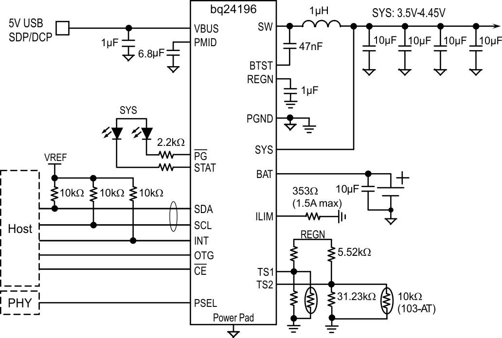
6 Pin Configuration and Functions
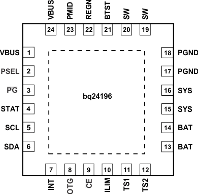
Pin Functions
| PIN | TYPE | DESCRIPTION | |
|---|---|---|---|
| NAME | NUMBER | ||
| VBUS | 1,24 | P | Charger Input Voltage. The internal n-channel reverse block MOSFET (RBFET) is connected between VBUS and PMID with VBUS on source. Place a 1-µF ceramic capacitor from VBUS to PGND and place it as close as possible to IC. (Refer to Application Information Section for details) |
| PSEL | 2 | I Digital |
Power source selection input. High indicates a USB host source and Low indicates an adapter source. |
| PG | 3 | O Digital |
Open drain active low power good indicator. Connect to the pull up rail via 10-kΩ resistor. LOW indicates a good input source if the input voltage is between UVLO and ACOV, above SLEEP mode threshold, and current limit is above 30 mA. |
| STAT | 4 | O Digital |
Open drain charge status output to indicate various charger operation. Connect to the pull up rail via 10-kΩ. LOW indicates charge in progress. HIGH indicates charge complete or charge disabled. When any fault condition occurs, STAT pin blinks at 1 Hz. |
| SCL | 5 | I Digital |
I2C Interface clock. Connect SCL to the logic rail through a 10-kΩ resistor. |
| SDA | 6 | I/O Digital |
I2C Interface data. Connect SDA to the logic rail through a 10-kΩ resistor. |
| INT | 7 | O Digital |
Open-drain Interrupt Output. Connect the INT to a logic rail via 10-kΩ resistor. The INT pin sends active low, 256-us pulse to host to report charger device status and fault. |
| OTG | 8 | I Digital |
USB current limit selection pin during buck mode, and active high enable pin during boost mode. |
| In buck mode with USB host (PSEL=High), when OTG = High, IIN limit = 500 mA and when OTG = Low, IIN limit = 100 mA. | |||
| The boost mode is activated when the REG01[5:4] = 10 and OTG pin is High. | |||
| CE | 9 | I Digital |
Active low Charge Enable pin. Battery charging is enabled when REG01[5:4] = 01 and CE pin = Low. CE pin must be pulled high or low. |
| ILIM | 10 | I Analog |
ILIM pin sets the maximum input current limit by regulating the ILIM voltage at 1 V. A resistor is connected from ILIM pin to ground to set the maximum limit as IINMAX = (1V/RILIM) × 530. The actual input current limit is the lower one set by ILIM and by I2C REG00[2:0]. The minimum input current programmed on ILIM pin is 500 mA. |
| TS1 | 11 | I Analog |
Temperature qualification voltage input #1. Connect a negative temperature coefficient thermistor. Program temperature window with a resistor divider from REGN to TS1 to GND. Charge suspends when either TS pin is out of range. Recommend 103AT-2 thermistor. |
| TS2 | 12 | I Analog |
Temperature qualification voltage input #2. Connect a negative temperature coefficient thermistor. Program temperature window with a resistor divider from REGN to TS2 to GND. Charge suspends when either TS pin is out of range. Recommend 103AT-2 thermistor. TS1 and TS2 pin can be connected together for single thermistor application. |
| BAT | 13,14 | P | Battery connection point to the positive terminal of the battery pack. The internal BATFET is connected between BAT and SYS. Connect a 10 µF closely to the BAT pin. |
| SYS | 15,16 | P | System connection point. The internal BATFET is connected between BAT and SYS. When the battery falls below the minimum system voltage, switch-mode converter keeps SYS above the minimum system voltage. (Refer to Application Information Section for inductor and capacitor selection.) |
| PGND | 17,18 | P | Power ground connection for high-current power converter node. Internally, PGND is connected to the source of the n-channel LSFET. On PCB layout, connect directly to ground connection of input and output capacitors of the charger. A single point connection is recommended between power PGND and the analog GND near the IC PGND pin. |
| SW | 19,20 | O Analog |
Switching node connecting to output inductor. Internally SW is connected to the source of the n-channel HSFET and the drain of the n-channel LSFET. Connect the 0.047-µF bootstrap capacitor from SW to BTST. |
| BTST | 21 | P | PWM high side driver positive supply. Internally, the BTST is connected to the anode of the boost-strap diode. Connect the 0.047-µF bootstrap capacitor from SW to BTST. |
| REGN | 22 | P | PWM low side driver positive supply output. Internally, REGN is connected to the cathode of the boost-strap diode. Connect a 4.7-µF (10-V rating) ceramic capacitor from REGN to analog GND. The capacitor should be placed close to the IC. REGN also serves as bias rail of TS1 and TS2 pins. |
| PMID | 23 | O Analog |
Connected to the drain of the reverse blocking MOSFET and the drain of HSFET. Given the total input capacitance, connect a 1-µF capacitor on VBUS to PGND, and the rest all on PMID to PGND. (Refer to Application Information Section for details) |
| Thermal Pad | – | P | Exposed pad beneath the IC for heat dissipation. Always solder thermal pad to the board, and have vias on the thermal pad plane star-connecting to PGND and ground plane for high-current power converter. |
7 Specifications
7.1 Absolute Maximum Ratings(1)
over operating free-air temperature range (unless otherwise noted)| MIN | MAX | UNIT | ||
|---|---|---|---|---|
| Voltage range (with respect to GND) | VBUS | –2 | 22 | V |
| PMID | –0.3 | 22 | V | |
| STAT, PG | –0.3 | 20 | V | |
| BTST | –0.3 | 26 | V | |
| SW | –2 | 20 | V | |
| BAT, SYS (converter not switching) | –0.3 | 6 | V | |
| SDA, SCL, INT, OTG, ILIM, REGN, TS1, TS2, CE, PSEL | –0.3 | 7 | V | |
| BTST TO SW | –0.3 | –7 | V | |
| PGND to GND | –0.3 | –0.3 | V | |
| Output sink current | INT, STAT, PG | 6 | mA | |
| Junction temperature | –40°C | 150 | °C | |
| Storage temperature, Tstg | –65 | 150 | °C | |
7.2 ESD Ratings
| VALUE | UNIT | |||
|---|---|---|---|---|
| V(ESD) | Electrostatic discharge | Human body model (HBM), per ANSI/ESDA/JEDEC JS-001(1) | 1000 | V |
| Charged device model (CDM), per JEDEC specification JESD22-C101(2) | 250 | |||
7.3 Recommended Operating Conditions
| MIN | MAX | UNIT | ||
|---|---|---|---|---|
| VIN | Input voltage | 3.9 | 17(1) | V |
| IIN | Input current | 3 | A | |
| ISYS | Output current (SYS) | 2.5 | A | |
| VBAT | Battery voltage | 4.4 | V | |
| IBAT | Fast charging current | 2.5 | A | |
| Discharging current with internal MOSFET | 6 (continuous) 9 (peak) (up to 1 sec duration) |
A | ||
| TA | Operating free-air temperature range | –40 | 85 | °C |
7.4 Thermal Information
| THERMAL METRIC(1) | bq24196 | UNIT | |
|---|---|---|---|
| RGE (24 PIN) | |||
| RθJA | Junction-to-ambient thermal resistance | 32.2 | °C/W |
| RθJCtop | Junction-to-case (top) thermal resistance | 29.8 | |
| RθJB | Junction-to-board thermal resistance | 9.1 | |
| ψJT | Junction-to-top characterization parameter | 0.3 | |
| ψJB | Junction-to-board characterization parameter | 9.1 | |
| RθJCbot | Junction-to-case (bottom) thermal resistance | 2.2 | |
7.5 Electrical Characteristics
VVBUS_UVLOZ < VVBUS < VACOV and VVBUS > VBAT + VSLEEP, TJ = –40°C to 125°C and TJ = 25°C for typical values unless other noted.7.6 Typical Characteristics
Table 1. Table of Figures
| FIGURE NO. | |
|---|---|
| System Light Load Efficiency vs System Load Current | Figure 1 |
| SYS Voltage Regulation vs System Load | Figure 2 |
| Charging Efficiency vs Charging Current | Figure 3 |
| Boost Mode Efficiency vs VBUS Load Current | Figure 4 |
| Boost Mode VBUS Voltage Regulation vs VBUS Load Current | Figure 5 |
| SYS Voltage vs Temperature | Figure 6 |
| BAT Voltage vs Temperature | Figure 7 |
| Input Current Limit vs Temperature | Figure 8 |
| Charge Current vs Temperature | Figure 9 |


