SLUS821J October 2008 – May 2017
PRODUCTION DATA.
- 1 Features
- 2 Applications
- 3 Description
- 4 Revision History
- 5 Device Comparison Table
- 6 Pin Configuration and Functions
- 7 Specifications
-
8 Detailed Description
- 8.1 Overview
- 8.2 Functional Block Diagram
- 8.3 Feature Description
- 8.4 Device Functional Modes
-
9 Application and Implementation
- 9.1 Application Information
- 9.2
Typical Applications
- 9.2.1 Using The bq24232 In A Stand-Alone Charger Application
- 9.2.2 Using The bq24230 in a Host Controlled Charger Application
- 10Power Supply Recommendations
- 11Layout
- 12Device and Documentation Support
- 13Mechanical, Packaging, and Orderable Information
パッケージ・オプション
メカニカル・データ(パッケージ|ピン)
- RGT|16
サーマルパッド・メカニカル・データ
- RGT|16
発注情報
8 Detailed Description
8.1 Overview
The bq2423x devices are integrated Li-ion linear chargers and system power-path management devices targeted at space-limited portable applications. The device powers the system while simultaneously and independently charging the battery. This feature reduces the number of charge and discharge cycles on the battery, allows for proper charge termination, and enables the system to run with a defective or absent battery pack. It also allows instant system turnon even with a totally discharged battery. The input power source for charging the battery and running the system can be an AC adapter or a USB port. The devices feature dynamic power-path management (DPPM), which shares the source current between the system and battery charging and automatically reduces the charging current if the system load increases. When charging from a USB port, the input dynamic power management (VIN-DPM) circuit reduces the input current limit if the input voltage falls below a threshold, preventing the USB port from crashing. The power-path architecture also permits the battery to supplement the system current requirements when the adapter cannot deliver the peak system currents.
8.2 Functional Block Diagram
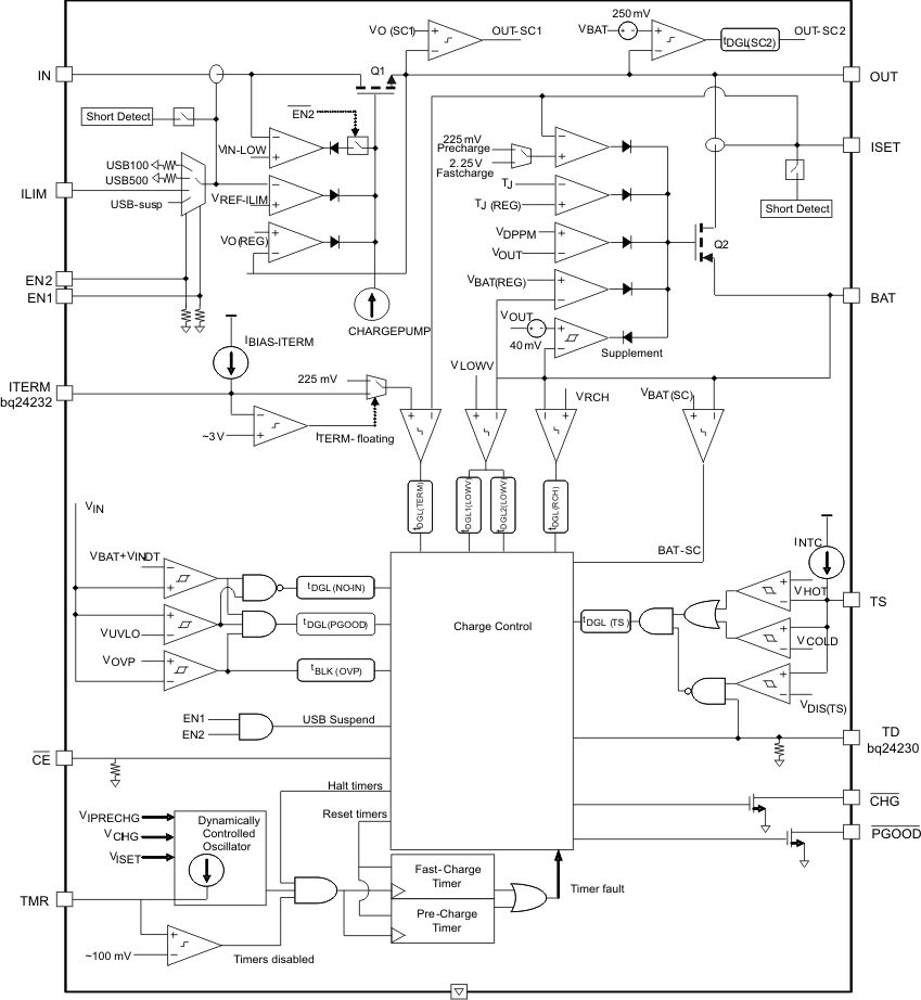
8.3 Feature Description
8.3.1 Undervoltage Lockout
The bq2423x family remains in power-down mode when the input voltage at the IN pin is below the undervoltage lockout (UVLO) threshold.
During the power-down mode, the host commands at the control inputs (CE, EN1 and EN2) are ignored. The Q1 FET connected between IN and OUT pins is off, and the status outputs CHG and PGOOD are high impedance. The Q2 FET that connects BAT to OUT is ON. During power-down mode, the VOUT(SC2) circuitry is active and monitors for overload conditions on OUT.
8.3.2 Power On
When VIN exceeds the UVLO threshold, the bq2423x powers up. While VIN is below VBAT + VIN(DT), the host commands at the control inputs (CE, EN1, and EN2) are ignored. The Q1 FET connected between IN and OUT pins is off, and the status outputs CHG and PGOOD are high impedance. The Q2 FET that connects BAT to OUT is ON. During this mode, the VOUT(SC2) circuitry is active and monitors for overload conditions on OUT.
When VIN rises above VBAT + VIN(DT), PGOOD is low to indicate that the valid power status and the CE, EN1, and EN2 inputs are read. The device enters standby mode whenever (EN1, EN2) = (1, 1) or if an input overvoltage condition occurs. In standby mode, Q1 is OFF and Q2 is ON. During standby mode, the VOUT(SC2) circuitry is active and monitors for overload conditions on OUT.
When the input voltage at IN is within the valid range: VIN > UVLO AND VIN > VBAT + VIN(DT) AND VIN < VOVP, and the EN1 and EN2 pins indicate that the USB suspend mode is not enabled [(EN1, EN2) ≠ (HI, HI)], all internal timers and other circuit blocks are activated. The device checks for short circuits at the ISET and ILIM pins. If no short conditions exists, the device switches on the input FET Q1 with a 100-mA current limit to check for a short circuit at OUT. If VOUT rises above VSC, the FET Q1 switches to the current-limit threshold set by EN1, EN2, and RILIM and the device enters normal operation where the system is powered by the input source (Q1 is on), and the device continuously monitors the status of CE, EN1, and EN2 as well as the input voltage conditions.
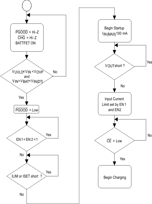 Figure 11. Start-Up Flow Diagram
8.3.3 Power-Path Management
The bq2423x features an OUT output that powers the external load connected to the battery. This output is active whenever a source is connected to IN or BAT. The following sections discuss the behavior of OUT with a source connected to IN to charge the battery and a battery source only.
8.3.3.1 Input Source Connected – Adapter or USB
With a source connected, the power-path management circuitry of the bq2423x monitors the input current continuously. The OUT output is regulated to a fixed voltage (VO(REG)). The current into IN is shared between charging the battery and powering the system load at OUT. The bq2423x has internal selectable current limits of 100 mA (USB100) and 500 mA (USB500) for charging from USB ports, as well as a resistor-programmable input current limit. See Table 1 for EN1, EN2 setting.
The bq2423x is USB-IF compliant for the inrush current testing. The USB spec allows up to 10 μF to be hard-started, which establishes 50 μF as the maximum inrush charge value when exceeding 100 mA. The input current limit for the bq2423x prevents the input current from exceeding this limit, even with system capacitances greater than 10 μF. Note that the input capacitance to the device must be selected small enough to prevent a violation (<10 μF), as this current is not limited.
The input current limit selection is controlled by the state of the EN1 and EN2 pins as shown in Table 1. When using the resistor-programmable current limit, the input current limit is set by the value of the resistor connected from the ILIM pin to VSS and is given by the Equation 1:
The input current limit is adjustable up to 500 mA. The valid resistor range is 2.75 kΩ to 8.4 kΩ.
When the IN source is connected, priority is given to the system load. The DPPM and Battery Supplement modes are used to maintain the system load. Figure 12 illustrates examples of the DPPM and supplement modes. These modes are explained in detail in the following sections.
8.3.3.1.1 Input Voltage Dynamic Power Management, (VIN_DPM)
The bq2423x uses the VIN_DPM mode for operation from current-limited sources (including USB ports). The input voltage is monitored and compared to the VIN-DPM threshold (nominally ~ 4.5V). If the adaptor input voltage begins to collapse, the input current limit is reduced to prevent the supply voltage from falling further. This prevents the bq2423x from crashing the external power source in case of a current-limited supply regardless of the input current limit setting (USB100, USB500, or external resistor-set ILIM mode)..
8.3.3.1.2 Dynamic Power Path Management (DPPM)
When the sum of the charging (BAT) and system (OUT) currents exceeds the preset maximum input current (programmed with EN1, EN2, and ILIM pins), the voltage at the OUT pin decreases. Once the voltage on the OUT pin falls to the VDPPM limit, the bq2423x enters DPPM mode. In this mode, the charging current is reduced and power to the system is prioritized. Battery termination is disabled and the charge timer period is extended while in DPPM mode, because the charging current is less than the programmed value.
8.3.3.1.3 Battery Supplement Mode
If the system load current demand exceeds the input current limit, even with charging current reduced to zero, the OUT voltage continues to drop. When the OUT pin voltage drops below VBSUP1, the partially charged battery supplements the external power source to provide current to the system. When the OUT pin voltage increases above VBSUP2 the device exits battery supplement mode and all system current is drawn from the external power source.
During supplement mode, the battery supplement current is not regulated; however, a short-circuit protection circuit is built in. If during battery supplement mode, the voltage at OUT drops 250 mV below the BAT voltage, the OUT output is turned off if the overload exists after tDGL(SC2). The short-circuit recovery timer then starts counting. After tREC(SC2), OUT turns on and attempts to restart. If the short circuit remains, OUT is turned off and the counter restarts. Battery termination is disabled while in supplement mode.
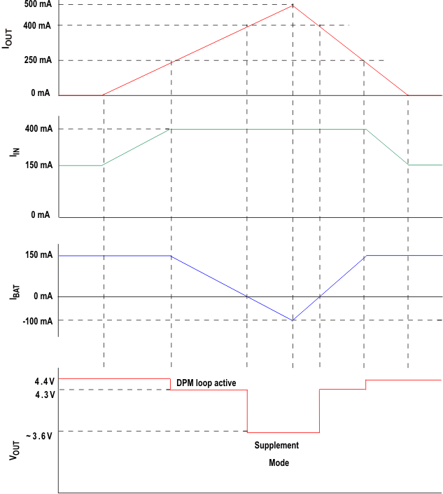 Figure 12. bq2423x DPPM And Battery Supplement Modes
(VOREG = 4.4 V, VBAT = 3.6 V, ILIM=400 mA, ICHG = 150 mA)
8.3.3.2 Input Source Not Connected
When no source is connected to the IN input, OUT is powered strictly from the battery. During this mode, the current into OUT is unregulated, similar to Battery Supplement Mode; however, the short-circuit circuitry is active. If the OUT voltage falls below the BAT voltage by 250 mV for longer than tDGL(SC2), OUT is turned off. The short-circuit recovery timer then starts counting. After tREC(SC2), OUT turns on and attempts to restart. If the short-circuit remains, OUT is turned off and the counter restarts. This ON/OFF cycle continues until the overload condition is removed.
8.3.4 Thermal Regulation and Thermal Shutdown
The bq2423x contain a thermal regulation loop that monitors the die temperature. If the die temperature exceeds TJ(REG), the device automatically reduces the charging current to prevent the die temperature from increasing further. In some cases, the die temperature continues to rise despite the operation of the thermal loop, particularly under high VIN and heavy OUT system load conditions. Under these conditions, if the die temperature increases to TJ(OFF), the input FET Q1 is turned OFF. FET Q2 is turned ON to ensure that the battery still powers the load on OUT. Once the device die temperature cools by TJ(OFF-HYS), the input FET Q1 is turned on and the device returns to thermal regulation. Continuous overtemperature conditions result in a hiccup mode. Safety timers are slowed proportionally to the charge current in thermal regulation. Battery termination is disabled during thermal regulation and thermal shutdown.
Note that this feature monitors the die temperature of the bq2423x. This is not synonymous with ambient temperature. Self-heating exists due to the power dissipated in the IC because of the linear nature of the battery charging algorithm and the LDO mode for OUT.
A modified charge cycle with the thermal loop active is shown in Figure 13:
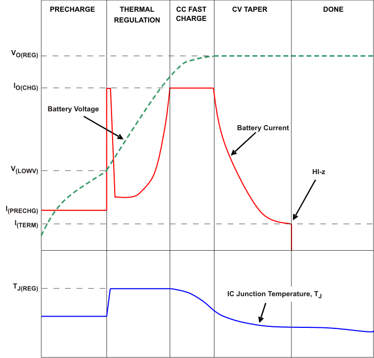 Figure 13. Modified Charge Cycle
8.3.5 Battery Pack Temperature Monitoring
The bq2423x features an external battery pack temperature monitoring input. The TS input connects to the NTC resistor in the battery pack to monitor battery temperature and prevent dangerous over-temperature conditions. Using the basic connection as shown in the Typical Application Circuit example on page 1, a nominal range of 0° to 50°C is achieved using a standard 103AT – 2 type thermistor (ß = 3435) with no additional external components.
During charging, INTC is sourced to TS and the voltage at TS is continuously monitored. If, at any time, the voltage at TS is outside of the operating range (VCOLD to VHOT), charging is suspended. The timers maintain their values but suspend counting. When the voltage measured at TS returns to within the operation window, charging is resumed and the timers continue counting. When charging is suspended due to a battery pack temperature fault, the CHG pin remains low and continues to indicate charging
For the bq24230, battery pack temperature sensing is disabled when termination is disabled (TD = High) and the voltage at TS is greater than VDIS(TS). The battery pack temperature monitoring is disabled in all devices by connecting a fixed 10-kΩ resistor from TS to VSS so that the voltage at the TS pin is always within the voltage range to permit charging.
8.3.5.1 Modifying / Extending the Allowable Temperature Range for Charging
The nominal temperature range to allow charging is 0°C to 50°C when using a typical 103AT-2 type thermistor. However, the user can increase the range by adding two external resistors. See Figure 14 for the circuit. The values for Rs and Rp are calculated using the following equations:


Where:
RTH: Thermistor Hot Trip Value found in thermistor data sheet
RTC: Thermistor Cold Trip Value found in thermistor data sheet
VH: Hot Trip Threshold of the IC = 0.3 V nominal
VC: Cold Trip Threshold of the IC = 2.1 V nominal
ITS: Output Current Bias of the IC = 75 µA nominal
NTC Thermsitor Semitec 103AT-2 Type or equivalent
Table 2 provides examples of the thermistor resistance at different temperatures and suggested typical Rs and Rp values, using 1% tolerance resistors that can extend the allowable temperature range beyond the standard 0°C – to – 50° C window.
Table 2. Example Thermistor Resistance and Suggested Typical Rs and Rp Values
| COLD TEMP RESISTANCE AND TRIP THRESHOLD; Ω (°C) |
HOT TEMP RESISTANCE AND TRIP THRESHOLD; Ω (°C) |
EXTERNAL BIAS RESISTOR, Rs (Ω) | EXTERNAL BIAS RESISTOR, Rp (Ω) |
|---|---|---|---|
| 28000 (–0.6) | 4000 (51) | 0 | ∞ |
| 28480 (–1) | 3536 (55) | 487 | 845000 |
| 28480 (–1) | 3021 (60) | 1000 | 549000 |
| 33890 (–5) | 4026 (51) | 76.8 | 158000 |
| 33890 (–5) | 3536 (55) | 576 | 150000 |
| 33890 (–5) | 3021 (60) | 1100 | 140000 |
RHOT and RCOLD are the thermistor resistance at the desired hot and cold temperatures, respectively. Note that the temperature window cannot be tightened more using the thermistor connected to TS, it can only be extended.
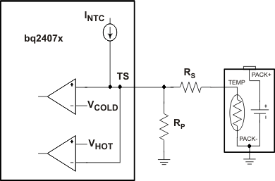 Figure 14. Extended TS Temperature Thresholds
8.4 Device Functional Modes
8.4.1 Battery Charging
Set CE low to initiate battery charging. First, the device checks for a short circuit on the BAT pin by sourcing IBAT(SC) to the battery and monitoring the voltage. When the BAT voltage exceeds VBAT(SC), the battery charging continues. The battery is charged in three phases: conditioning precharge, constant-current fast charge (current regulation), and a constant-voltage tapering (voltage regulation). In all charge phases, an internal control loop monitors the IC junction temperature and reduces the charge current if an internal temperature threshold is exceeded.
Figure 15 illustrates a normal Li-ion charge cycle using the bq2423x:
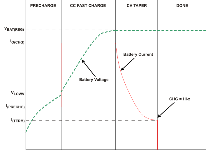 Figure 15. Normal Li-Ion Charge Cycle
In the precharge phase, the battery is charged with the precharge current (IPRECHG). Once the battery voltage crosses the VLOWV threshold, the battery is charged with the fast-charge current (ICHG). As the battery voltage reaches VBAT(REG), the battery is held at a constant voltage of VBAT(REG) and the charge current tapers off as the battery approaches full charge. When the battery current reaches ITERM, the CHG pin indicates charging done by going high impedance.
Note that termination detection is disabled whenever the charge rate is reduced because of the actions of the thermal loop, the DPPM loop, or the VIN(LOW) loop.
The value of the fast-charge current is set by the resistor connected from the ISET pin to VSS, and is given by the equation:
The charge current limit is adjustable from 25 mA to 500 mA. The valid resistor range is 1.8 kΩ to 36 kΩ. Note that if ICHG is programmed as greater than the input current limit, the battery does not charge at the rate of ICHG, but at the slower rate of IIN(MAX) (minus the load current on the OUT pin, if any). In this case, the charger timers are proportionately slowed down.
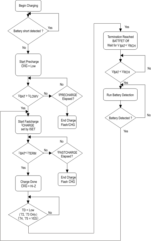 Figure 16. Battery Charging Flow Diagram
8.4.1.1 Charge Current Translator
When the charger is enabled, internal circuits generate a current proportional to the charge current at the ISET input. The current out of ISET is 1/400 (±10%) of the charge current. This current, when applied to the external charge current programming resistor, RISET, generates an analog voltage that can be monitored by an external host to calculate the current sourced from BAT.
8.4.1.2 Battery Detection and Recharge
The bq2423x automatically detects if a battery is connected or removed. Once a charge cycle is complete, the battery voltage is monitored. When the battery voltage falls below VRCH, the battery detection routine is run. The detection routine first applies IBAT(DET) for tDET to see if VBAT drops below VLOWV. If not, it indicates that the battery is still connected, but has discharged. If CE is low, the charger is turned on again to top off the battery. During this recharge cycle, the CHG output remains high-impedance as recharge cycles are not indicated by the CHG pin. If the BAT voltage falls below VLOWV during the battery detection test, it indicates that the battery has been removed or the protector is open. Next, the precharge current is applied for tDET to close the protector if possible. If the battery voltage does not rise above VRCH, it indicates that the protector is closed, or a battery has been inserted, and a new charge cycle begins. If the voltage rises above VRCH, the battery is determined missing and the detection routine continues. The battery detection runs until a battery is detected.
8.4.1.3 Termination Disable (TD Input, bq24230)
The bq24230 contains a TD input that allows termination to be enabled/disabled. Connect TD to a logic high to disable charge termination. When termination is disabled, the device goes through the precharge, fast-charge, and CV phases, then remains in the CV phase. During the CV phase, the charger maintains the output voltage at BAT equal to VBAT(REG), and charging current does not terminate. BAT sources currents up to ICHG or IIN-MAX, whichever is less. Battery detection is not performed. The CHG output is high impedance once the current falls below ITERM and does not go low until the input power or CE are toggled. When termination is disabled, the precharge and fast-charge safety timers are also disabled. Battery pack temperature sensing (TS pin functionality) is also disabled if the TD pin is high and the TS pin is unconnected.
8.4.1.4 Adjustable Termination Threshold (ITERM Input, bq24232)
The termination current threshold for the bq24232 is user-programmable. Set the termination current by connecting a resistor from ITERM to VSS. For USB100, mode (EN1 = EN2 = VSS), the termination current value is calculated as:
In the other input current limit modes (EN1 ≠ EN2), the termination current value is calculated as:
The termination current is programmable up to 50% of the fast-charge current. The RITERM resistor must be less than 15 kΩ. Leave ITERM unconnected to select the default internally set termination current.
8.4.1.5 Dynamic Charge Timers (TMR Input)
The bq2423x devices contain internal safety timers for the precharge and fast-charge phases to prevent potential damage to the battery and the system. The timers begin at the start of the respective charge cycles. The timer values are programmed by connecting a resistor from TMR to VSS. The resistor value is calculated using the following equation:
Leave TMR unconnected to select the internal default timers. Disable the timers by connecting TMR to VSS. Reset the timers by toggling CE pin.
Note that timers are suspended when the device is in thermal shutdown, and the timers are slowed proportionally to the charge current when the device enters thermal regulation. For the bq24230, the timers are disabled when TD is connected to a high logic level.
During the fast-charge phase, several events increase the timer durations.
- The system load current activates the DPPM loop which reduces the available charging current
- The input current is reduced because the input voltage has fallen to VIN(LOW)
- The device has entered thermal regulation because the IC junction temperature has exceeded TJ(REG)
During each of these events, the internal timers are slowed down proportionately to the reduction in charging current. For example, if the charging current is reduced by half for two minutes, the timer clock is reduced to half the frequency and the counter counts half as fast resulting in only one minute of counted time.
8.4.1.6 Status Indicators (PGOOD, CHG)
The bq2423x contains two open-drain outputs that signal its status. The PGOOD output signals when a valid input source is connected. PGOOD is low when (VBAT + VIN(DT)) < VIN < VOVP. When the input voltage is outside of this range, PGOOD is high impedance.
The CHG output signals when a new charge cycle is initiated. After a charge cycle is initiated, CHG goes low once the battery is above the short-circuit threshold. CHG goes high impedance once the charge current falls below ITERM. CHG remains high impedance until the input power is removed and reconnected or the CE pin is toggled. It does not signal subsequent recharge cycles.
Table 3. PGOOD Status Indicator
| Input State | PGOOD Output | |||
|---|---|---|---|---|
| VIN < VUVLO | Hi impedance | |||
| VUVLO < VIN < VIN(DT) + VBAT | Hi impedance | |||
| VIN(DT) + VBAT < VIN < VOVP | Low | |||
| VIN > VOVP | Hi impedance | |||
Table 4. CHG Status Indicator
| Charge State | CHG Output | |||
|---|---|---|---|---|
| Charging | Low (first charge cycle) | |||
| Charging terminated | Hi impedance until power or CE is toggled | |||
| Recharging after termination | Hi impedance | |||
| Carging suspended by thermal loop | Low (first charge cycle) | |||
| Safety timers expired | Flashing at 2Hz | |||
| IC disabled or no valid input power | Hi impedance | |||
8.4.1.6.1 Timer Fault
If the precharge timer expires before the battery voltage reaches VLOWV, the bq2423x indicates a fault condition. Additionally, if the battery current does not fall to ITERM before the fast-charge timer expires, a fault is indicated. The CHG output flashes at approximately 2 Hz to indicate a fault condition.
8.4.2 Explanation of Deglitch Times and Comparator Hysteresis
Figures not to scale
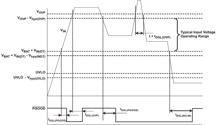 Figure 17. Power Up, Power Down
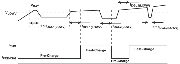 Figure 18. Pre- To Fast-Charge, Fast- To Precharge Transition – TDGL1(LOWV), TDGL2(LOWV)
 Figure 19. Recharge – TDGL(RCH)
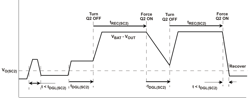 Figure 20. Out Short-Circuit – Supplement Mode
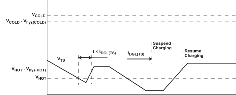 Figure 21. Battery Pack Temperature Sensing – TS Pin. Battery Temperature Increasing