SLUSBY5G June 2014 – December 2015
UNLESS OTHERWISE NOTED, this document contains PRODUCTION DATA.
- 1 Features
- 2 Applications
- 3 Description
- 4 Revision History
- 5 Pin Configuration and Functions
- 6 Specifications
-
7 Detailed Description
- 7.1 Overview
- 7.2 Functional Block Diagram
- 7.3 Feature Description
- 7.4
Device Functional Modes
- 7.4.1 High Impedance Mode
- 7.4.2 Battery Only Connected
- 7.4.3 Input Connected
- 7.4.4 Battery Charging Process
- 7.4.5 Charge Time Optimizer
- 7.4.6 Battery Detection
- 7.4.7 Battery Overvoltage Protection (BOVP)
- 7.4.8 Dynamic Power Path Management
- 7.4.9 Battery Discharge FET (BGATE)
- 7.4.10 IUSB1, IUSB2, and IUSB3 Input
- 7.4.11 Safety Timer in Charge Mode
- 7.4.12 LDO Output (DRV)
- 7.4.13 External NTC Monitoring (TS)
- 7.4.14 Thermal Regulation and Protection
- 7.4.15 Status Outputs (CHG, PG)
- 7.4.16 Boost Mode Operation
- 8 Applications and Implementation
- 9 Power Supply Recommendations
- 10Layout
- 11Device and Documentation Support
- 12Mechanical, Packaging, and Orderable Information
8 Applications and Implementation
NOTE
Information in the following applications sections is not part of the TI component specification, and TI does not warrant its accuracy or completeness. TI’s customers are responsible for determining suitability of components for their purposes. Customers should validate and test their design implementation to confirm system functionality.
8.1 Application Information
The bq24266EVM-609 evaluation module (EVM) is a complete charger module for evaluating the bq24266. The application curves were taken using the bq24266EVM-609 (SLUUB40). See Related Documentation.
The bq24266EVM is shipped with the bq24266 populated, For the bq24266, the TS input is available and the resistors are chosen using Equation 3 and Equation 4.
8.2 Typical Applications
8.2.1 Typical Application, External Discharge FET
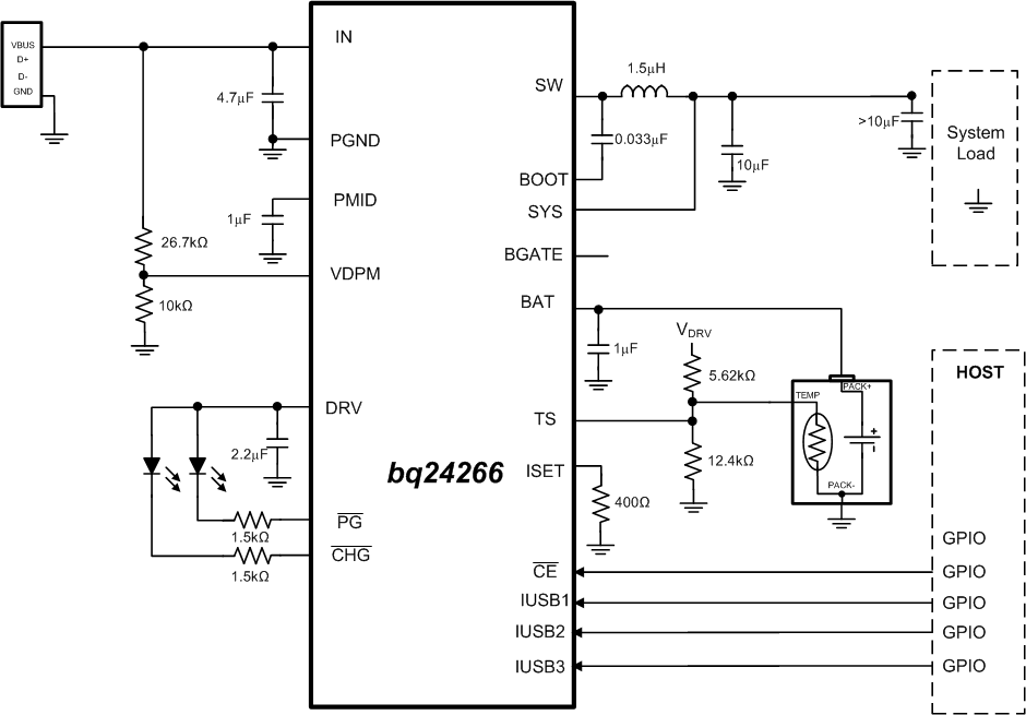 Figure 14. bq24266 Typical Application Circuit
8.2.1.1 Design Requirements
Table 4. Design Requirements
| DESIGN PARAMATER | EXAMPLE VALUE | |||
|---|---|---|---|---|
| Input Voltage Range | 4.75 V to 5.25 V nominal, withstand 28 V | |||
| Input Current Limit | 2500 mA | |||
| Input DPM Threshold | 4.2 V (Externally Set) | |||
| Fast Charge Current | 3000 mA | |||
| Battery Charge Voltage | 4.2 V | |||
| Termination Current | 300 mA | |||
8.2.1.2 Detailed Design Procedure
The parameters are configurable using the EVM jumper options as described in the Users Manual. The typical application for the bq24266EVM is shown in Figure 14. The default IUSB settings are for 2.5A input current limit and external VINDPM threshold, which is IUSB3 = 1, IUSB = 2 = 1, IUSB1 = 0. The VDPM resistors were selected using Equation 1. The charge current, ICHARGE, was set to be 3A using Equation 2.
The typical application circuit shows the minimum capacitance requirements for each pin. Options for sizing the inductor outside the 1.5 μH recommended value and additional SYS pin capacitance are explained in the next section. The resistors on PG and CHG are sized per each LED's current requirements. The TS resistor divider for configuring the TS function to work with the battery's specific thermistor can be computed from Equation 3 and Equation 4. The external battery FET is optional.
8.2.1.2.1 Output Inductor and Capacitor Selection Guidelines
When selecting an inductor, several attributes must be examined to find the right part for the application. First, the inductance value should be selected. The bq24266 is designed to work with 1.5µH to 2.2µH inductors. The chosen value will have an effect on efficiency and package size. Due to the smaller current ripple, some efficiency gain is reached using the 2.2µH inductor, however, due to the physical size of the inductor, this may not be a viable option. The 1.5µH inductor provides a good tradeoff between size and efficiency.
Once the inductance has been selected, the peak current must be calculated in order to choose the current rating of the inductor. Use Equation 7 to calculate the peak current.

The inductor selected must have a saturation current rating greater than or equal to the calculated IPEAK. Due to the high currents possible with the bq24266, a thermal analysis must also be done for the inductor. Many inductors have 40°C temperature rise rating. This is the DC current that will cause a 40°C temperature rise above the ambient temperature in the inductor. For this analysis, the typical load current may be used adjusted for the duty cycle of the load transients. For example, if the application requires a 1.5A DC load with peaks at 2.5A 20% of the time, a Δ40°C temperature rise current must be greater than 1.7A:
The internal loop compensation of the bq24266 is designed to be stable with 10µF to 150µF of local capacitance but requires at least 20µF total capacitance on the SYS rail (10µF local + ≥ 10µF distributed). The capacitance on the SYS rail can be higher than 150µF if distributed amongst the rail. To reduce the output voltage ripple, a ceramic capacitor with the capacitance between 10µF and 47µF is recommended for local bypass to SYS. If greater than 100µF effective capacitance is on the SYS rail, place at least 10µF bypass on the BAT pin. Pay special attention to the DC bias characteristics of ceramic capacitors. For small case sizes, the capacitance can be derated as high as 70% at workable voltages. All capacitances specified in this datasheet are effective capacitance, not capacitor value.
8.2.2 Application Curves
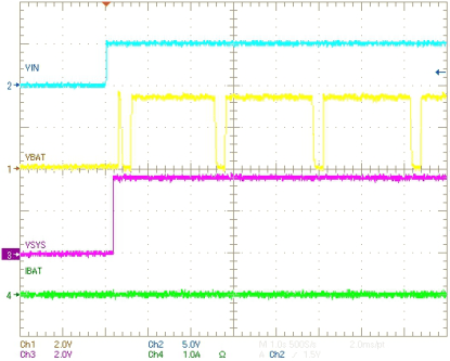 Figure 15. Startup With No Battery
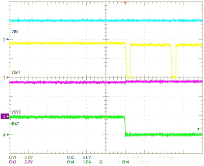 Figure 17. Battery Removal
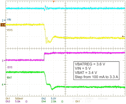 Figure 19. VSYS Transient With Supplement Mode
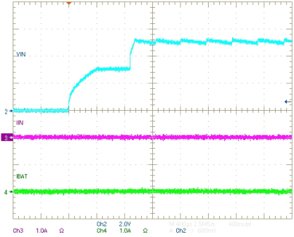 Figure 21. Boost Startup No Load
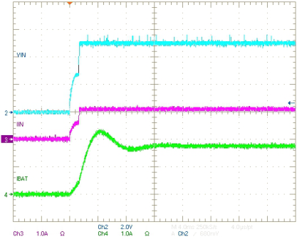 Figure 23. Boost Startup 1A Load
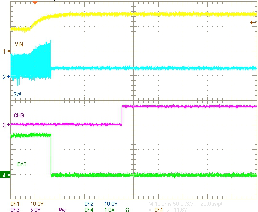 Figure 25. Input OVP Event with CHG
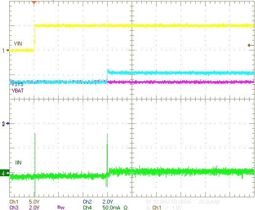
| VIN = 5 V |
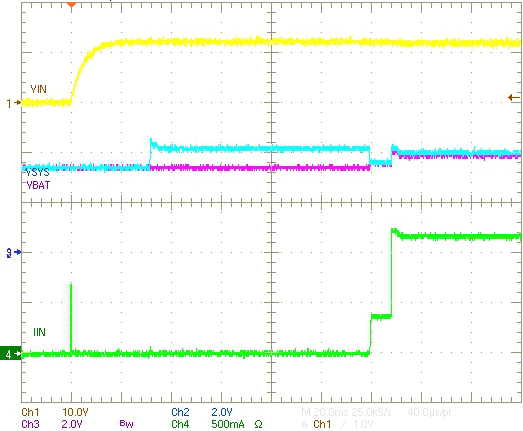
| VIN = 12 V |
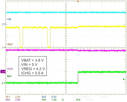 Figure 16. Battery Detection
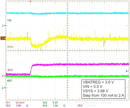 Figure 18. VSYS Transient Without Supplement Mode
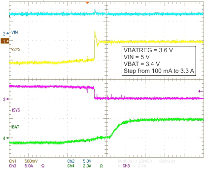 Figure 20. VSYS Transient With Supplement Mode
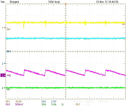 Figure 22. Boost Burst Mode During Light Load
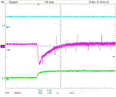 Figure 24. Boost Transient Response
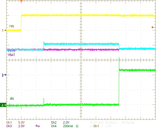
| VIN = 5 V |
