SLUS763D July   2007  – April 2016

PRODUCTION DATA.  

  1. Features
  2. Applications
  3. Description
  4. Revision History
  5. Pin Configuration and Functions
  6. Specifications
    1. 6.1 Absolute Maximum Ratings
    2. 6.2 ESD Ratings
    3. 6.3 Recommended Operating Conditions
    4. 6.4 Thermal Information
    5. 6.5 Electrical Characteristics
    6. 6.6 Timing Requirements
    7. 6.7 Typical Characteristics
  7. Detailed Description
    1. 7.1 Overview
    2. 7.2 Functional Block Diagram
    3. 7.3 Feature Description
      1. 7.3.1 Power Down
      2. 7.3.2 Power-On Reset
      3. 7.3.3 Operation
        1. 7.3.3.1 Input Overvoltage Protection
        2. 7.3.3.2 Input Overcurrent Protection
        3. 7.3.3.3 Battery Overvoltage Protection
        4. 7.3.3.4 Thermal Protection
        5. 7.3.3.5 Enable Function
        6. 7.3.3.6 Fault Indication
    4. 7.4 Device Functional Modes
      1. 7.4.1 OPERATION Mode
      2. 7.4.2 POWER-DOWN Mode
      3. 7.4.3 POWER-ON RESET Mode
  8. Applications and Implementation
    1. 8.1 Application Information
    2. 8.2 Typical Application
      1. 8.2.1 Design Requirements
      2. 8.2.2 Detailed Design Procedure
        1. 8.2.2.1 Selection of RBAT
        2. 8.2.2.2 Selection of RCE, RFAULT, and RPU
        3. 8.2.2.3 Selection of Input and Output Bypass Capacitors
      3. 8.2.3 Application Curves
  9. Power Supply Recommendations
    1. 9.1 Powering Accessories
  10. 10Layout
    1. 10.1 Layout Guidelines
    2. 10.2 Layout Example
  11. 11Device and Documentation Support
    1. 11.1 Related Links
    2. 11.2 Community Resources
    3. 11.3 Trademarks
    4. 11.4 Electrostatic Discharge Caution
    5. 11.5 Glossary
  12. 12Mechanical, Packaging, and Orderable Information

パッケージ・オプション

デバイスごとのパッケージ図は、PDF版データシートをご参照ください。

メカニカル・データ(パッケージ|ピン)
  • DSG|8
サーマルパッド・メカニカル・データ
発注情報

10 Layout

10.1 Layout Guidelines

  • This device is a protection device, and is meant to protect down-stream circuitry from hazardous voltages. Potentially, high voltages may be applied to this IC. It has to be ensured that the edge-to-edge clearances of PCB traces satisfy the design rules for high voltages.
  • The device uses SON packages with a PowerPAD™. For good thermal performance, the PowerPAD must be thermally coupled with the PCB ground plane. In most applications, this will require a copper pad directly under the IC. This copper pad must be connected to the ground plane with an array of thermal vias.
  • CIN and COUT must be located close to the IC. Other components like RILIM and RBAT should also be located close to the IC.

10.2 Layout Example
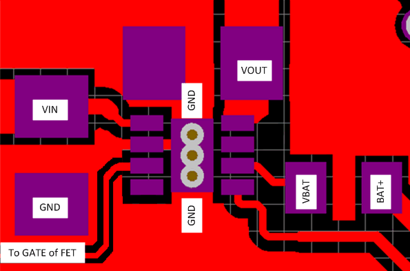
bq24314 bq24316 lus977_layout.gif Figure 27. Recommended Layout