SLUSAV3A August 2012 – July 2015
PRODUCTION DATA.
- 1 Features
- 2 Applications
- 3 Description
- 4 Revision History
- 5 Pin Configuration and Functions
- 6 Specifications
- 7 Detailed Description
- 8 Application and Implementation
- 9 Power Supply Recommendations
- 10Layout
- 11Device and Documentation Support
- 12Mechanical, Packaging, and Orderable Information
パッケージ・オプション
メカニカル・データ(パッケージ|ピン)
- DSG|8
サーマルパッド・メカニカル・データ
- DSG|8
発注情報
6 Specifications
6.1 Absolute Maximum Ratings
over operating free-air temperature range (unless otherwise noted)(1)| MIN | MAX | UNIT | |||
|---|---|---|---|---|---|
| VI | Input voltage | IN (with respect to VSS) | –0.3 | 30 | V |
| OUT (with respect to VSS) | –0.3 | 12 | |||
| ILIM, FAULT, CE, VBAT (with respect to VSS) | –0.3 | 7 | |||
| II | Input current | IN | 2 | A | |
| IO | Output current | OUT | 2 | A | |
| Output sink current | FAULT | 15 | mA | ||
| TJ | Junction temperature | –40 | 150 | °C | |
| Tstg | Storage temperature | –65 | 150 | °C | |
(1) Stresses beyond those listed under Absolute Maximum Ratings may cause permanent damage to the device. These are stress ratings only, which do not imply functional operation of the device at these or any other conditions beyond those indicated under Recommended Operating Conditions. Exposure to absolute-maximum-rated conditions for extended periods may affect device reliability.
6.2 ESD Ratings
| VALUE | UNIT | ||||
|---|---|---|---|---|---|
| V(ESD) | Electrostatic discharge | Human-body model (HBM), per ANSI/ESDA/JEDEC JS-001(1) | ±2000 | V | |
| Charged-device model (CDM), per JEDEC specification JESD22-C101(2) | ±500 | ||||
| IN(IEC 61000-4-2)(3) | Air Discharge | ±15000 | |||
| Contact | ±8000 | ||||
(1) JEDEC document JEP155 states that 500-V HBM allows safe manufacturing with a standard ESD control process.
(2) JEDEC document JEP157 states that 250-V CDM allows safe manufacturing with a standard ESD control process.
(3) With IN bypassed to the VSS with a 1-μF low-ESR ceramic capacitor
6.3 Recommended Operating Conditions
over operating free-air temperature range (unless otherwise noted)| MIN | NOM | MAX | UNIT | ||
|---|---|---|---|---|---|
| VIN | Input voltage range | 3 | 30 | V | |
| IIN | Input current, IN pin | 1.5 | A | ||
| IOUT | Output current, OUT pin | 1.5 | A | ||
| RILIM | OCP Programming resistor | 15 | 90 | kΩ | |
| TJ | Junction temperature | –40 | 125 | °C | |
6.4 Thermal Information
| THERMAL METRIC(1) | bq24314C | UNIT | |
|---|---|---|---|
| DSG (WSON) | |||
| 8 PINS | |||
| RθJA | Junction-to-ambient thermal resistance | 58.6 | °C/W |
| RθJC(top) | Junction-to-case (top) thermal resistance | 67.9 | °C/W |
| RθJB | Junction-to-board thermal resistance | 29.7 | °C/W |
| ψJT | Junction-to-top characterization parameter | 1.2 | °C/W |
| ψJB | Junction-to-board characterization parameter | 30.3 | °C/W |
| RθJC(bot) | Junction-to-case (bottom) thermal resistance | 7.6 | °C/W |
(1) For more information about traditional and new thermal metrics, see the Semiconductor and IC Package Thermal Metrics application report, SPRA953.
6.5 Electrical Characteristics
over operating free-air temperature range –40°C to +125°C and recommended supply voltage (unless otherwise noted)| PARAMETER | TEST CONDITIONS | MIN | TYP | MAX | UNIT | |||
|---|---|---|---|---|---|---|---|---|
| IN | ||||||||
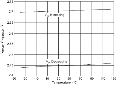
| UVLO | Undervoltage lock-out, input power detected threshold | CE = Low, VIN increasing from 0 V to 3 V | 2.6 | 2.7 | 2.8 | V | ||
| Vhys(UVLO) | Hysteresis on UVLO | CE = Low, VIN decreasing from 3 V to 0 V | 200 | 260 | 300 | mV | ||
| TDGL(PGOOD) | Deglitch time, input power detected status | CE = Low. Time measured from VIN 0 V → 5 V 1 μs rise-time, to output turning ON | 8 | ms | ||||
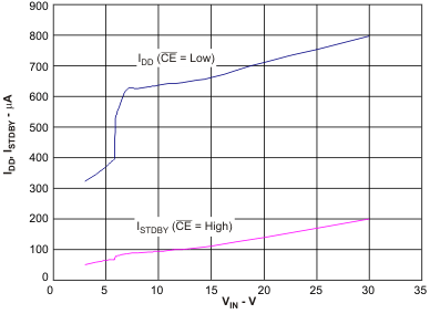
| IDD | Operating current | CE = Low, No load on OUT pin, VIN = 5 V, RILIM = 24.9 kΩ |
400 | 600 | μA | |||
| ISTDBY | Standby current | CE = High, VIN = 5 V | 65 | 95 | μA | |||
| INPUT TO OUTPUT CHARACTERISTICS | ||||||||
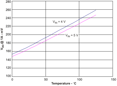
| VDO | Drop-out voltage IN to OUT | CE = Low, VIN = 5 V, IOUT = 1 A | 170 | 280 | mV | |||
| INPUT OVERVOLTAGE PROTECTION | ||||||||
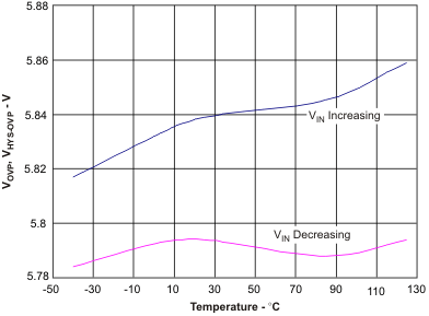
| VOVP | Input overvoltage protection threshold | CE = Low, VIN increasing from 5 V to 7.5 V | 5.71 | 5.85 | 6.00 | V | ||
| tPD(OVP) | Input OV propagation delay(1) | CE = Low | 200 | ns | ||||
| Vhys(OVP) | Hysteresis on OVP | CE = Low, VIN decreasing from 7.5 V to 5 V | 20 | 60 | 110 | mV | ||
| tON(OVP) | Recovery time from input overvoltage condition | CE = Low, Time measured from VIN 7.5 V → 5 V, 1 μs fall-time |
8 | ms | ||||
| INPUT OVERCURRENT PROTECTION | ||||||||
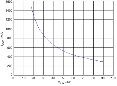
| IOCP | Input overcurrent protection threshold range | 300 | 1500 | mA | ||||
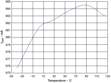
| IOCP | Input overcurrent protection threshold | CE = Low, RILIM = 24.9 kΩ, 3 V ≤ VIN < VOVP -Vhys(OVP) |
900 | 1000 | 1100 | mA | ||
| KILIM | Programmable current limit factor | 25 | AkΩ | |||||
| tBLANK(OCP) | Blanking time, input overcurrent detected | 176 | μs | |||||
| tREC(OCP) | Recovery time from input overcurrent condition | 64 | ms | |||||
| BATTERY OVERVOLTAGE PROTECTION | ||||||||
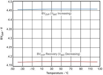
| BVOVP | Battery overvoltage protection threshold | CE = Low, VIN > 4.4 V | 4.4 | 4.45 | 4.5 | V | ||
| Vhys(Bovp) | Hysteresis on BVOVP | CE = Low, VIN > 4.4 V | 200 | 280 | 350 | mV | ||
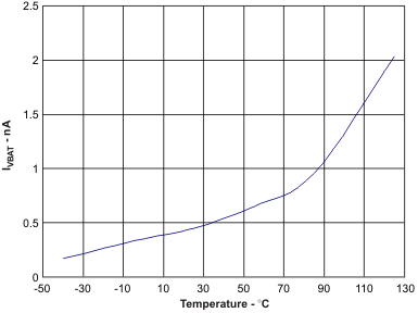
| IVBAT | Input bias current on VBAT pin | VBAT = 4.4 V, TJ = 25°C | 10 | nA | ||||
| TDGL(Bovp) | Deglitch time, battery overvoltage detected | CE = Low, VIN > 4.4 V. Time measured from VVBAT rising from 4.1 V to 4.4 V to FAULT going low. | 176 | μs | ||||
| THERMAL PROTECTION | ||||||||
| TJ(OFF) | Thermal shutdown temperature | 140 | 150 | °C | ||||
| TJ(OFF-HYS) | Thermal shutdown hysteresis | 20 | °C | |||||
| LOGIC LEVELS ONCE | ||||||||
| VIL | Low-level input voltage | 0 | 0.4 | V | ||||
| VIH | High-level input voltage | 1.4 | V | |||||
| IIL | Low-level input current | VCE = 0 V | 1 | μA | ||||
| IIH | High-level input current | VCE = 1.8 V | 15 | μA | ||||
| LOGIC LEVELS ONFAULT | ||||||||
| VOL | Output low voltage | ISINK = 5 mA | 0.2 | V | ||||
| IHI-Z | Leakage current, FAULT pin HI-Z | VFAULT = 5 V | 10 | μA | ||||
(1) Not tested in production. Specified by design.
6.6 Typical Characteristics
Test conditions (unless otherwise noted) for typical operating performance: VIN = 5 V, CIN = 1 μF, COUT = 1 μF, RILIM = 24.9 kΩ, RBAT = 100 kΩ, TA = 25°C, VPU = 3.3 V (see Figure 12 for the Typical Application Circuit)