JAJSBJ1B July 2010 – January 2020 BQ24650
PRODUCTION DATA.
- 1 特長
- 2 アプリケーション
- 3 概要
- 4 改訂履歴
- 5 概要(続き)
- 6 Pin Configuration and Functions
- 7 Specifications
-
8 Detailed Description
- 8.1 Overview
- 8.2 Functional Block Diagram
- 8.3
Feature Description
- 8.3.1 Battery Voltage Regulation
- 8.3.2 Input Voltage Regulation
- 8.3.3 Battery Current Regulation
- 8.3.4 Battery Precharge
- 8.3.5 Charge Termination and Recharge
- 8.3.6 Power Up
- 8.3.7 Enable and Disable Charging
- 8.3.8 Automatic Internal Soft-Start Charger Current
- 8.3.9 Converter Operation
- 8.3.10 Synchronous and Non-Synchronous Operation
- 8.3.11 Cycle-by-Cycle Charge Undercurrent
- 8.3.12 Input Overvoltage Protection (ACOV)
- 8.3.13 Input Undervoltage Lockout (UVLO)
- 8.3.14 Battery Overvoltage Protection
- 8.3.15 Cycle-by-Cycle Charge Overcurrent Protection
- 8.3.16 Thermal Shutdown Protection
- 8.3.17 Temperature Qualification
- 8.3.18 Charge Enable
- 8.3.19 Inductor, Capacitor, and Sense Resistor Selection Guidelines
- 8.3.20 Charge Status Outputs
- 8.3.21 Battery Detection
- 8.4 Device Functional Modes
- 9 Application and Implementation
- 10Power Supply Recommendations
- 11Layout
- 12デバイスおよびドキュメントのサポート
- 13メカニカル、パッケージ、および注文情報
パッケージ・オプション
メカニカル・データ(パッケージ|ピン)
- RVA|16
サーマルパッド・メカニカル・データ
- RVA|16
発注情報
8.3.17 Temperature Qualification
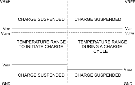
The controller continuously monitors battery temperature by measuring the voltage between the TS pin and GND. A negative temperature coefficient thermistor (NTC) and an external voltage divider typically develop this voltage. The controller compares this voltage against its internal thresholds to determine if charging is allowed. To initiate a charge cycle, the battery temperature must be within the VLTF to VHTF thresholds. If battery temperature is outside of this range, the controller suspends charge and waits until the battery temperature is within the VLTF to VHTF range. During the charge cycle the battery temperature must be within the VLTF to VTCO thresholds. If battery temperature is outside of this range, the controller suspends charge and waits until the battery temperature is within the VLTF to VHTF range. The controller suspends charge by turning off the PWM charge FETs. Figure 10 summarizes the operation.
 Figure 10. TS Pin, Thermistor Sense Thresholds
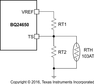
 Assuming a 103AT NTC thermistor on the battery pack as shown in Figure 15, the values of RT1 and RT2 can be determined by using Equation 7 and Equation 8:


 Figure 11. TS Resistor Network