JAJSBJ1B July 2010 – January 2020 BQ24650
PRODUCTION DATA.
- 1 特長
- 2 アプリケーション
- 3 概要
- 4 改訂履歴
- 5 概要(続き)
- 6 Pin Configuration and Functions
- 7 Specifications
-
8 Detailed Description
- 8.1 Overview
- 8.2 Functional Block Diagram
- 8.3
Feature Description
- 8.3.1 Battery Voltage Regulation
- 8.3.2 Input Voltage Regulation
- 8.3.3 Battery Current Regulation
- 8.3.4 Battery Precharge
- 8.3.5 Charge Termination and Recharge
- 8.3.6 Power Up
- 8.3.7 Enable and Disable Charging
- 8.3.8 Automatic Internal Soft-Start Charger Current
- 8.3.9 Converter Operation
- 8.3.10 Synchronous and Non-Synchronous Operation
- 8.3.11 Cycle-by-Cycle Charge Undercurrent
- 8.3.12 Input Overvoltage Protection (ACOV)
- 8.3.13 Input Undervoltage Lockout (UVLO)
- 8.3.14 Battery Overvoltage Protection
- 8.3.15 Cycle-by-Cycle Charge Overcurrent Protection
- 8.3.16 Thermal Shutdown Protection
- 8.3.17 Temperature Qualification
- 8.3.18 Charge Enable
- 8.3.19 Inductor, Capacitor, and Sense Resistor Selection Guidelines
- 8.3.20 Charge Status Outputs
- 8.3.21 Battery Detection
- 8.4 Device Functional Modes
- 9 Application and Implementation
- 10Power Supply Recommendations
- 11Layout
- 12デバイスおよびドキュメントのサポート
- 13メカニカル、パッケージ、および注文情報
パッケージ・オプション
メカニカル・データ(パッケージ|ピン)
- RVA|16
サーマルパッド・メカニカル・データ
- RVA|16
発注情報
9.2.2.6 MPPT Temperature Compensation
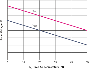
A typical solar panel comprises of a lot of cells in a series connection, and each cell is a forward-biased p-n junction. So, the open-circuit voltage (VOC) of a solar cell has a temperature coefficient that is similar to a common p-n diode, or about –2 mV/°C. A crystalline solar panel specification always provides both open-circuit voltage VOC and peak power point voltage VMP. The difference between VOC and VMP can be approximated as fixed and temperature-independent, so the temperature coefficient for the peak power point is similar to that of VOC. Normally, panel manufacturers specify the 25°C values for VOC and VMP, and the temperature coefficient for VOC, as shown in Figure 17.
 Figure 17. Solar Panel Output Voltage Temperature Characteristics
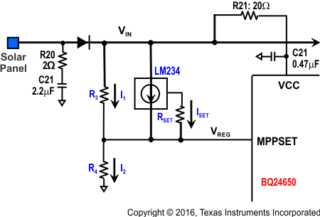
 The BQ24650 employs a feedback network to the MPPSET pin to program the input regulation voltage. Because the temperature characteristic for a typical solar panel VMP voltage is almost linear, a simple solution for tracking this characteristic can be implemented by using an LM234 3-terminal current source, which can create an easily programmable, linear temperature dependent current to compensate the negative temperature coefficient of the solar panel output voltage.
 Figure 18. Feedback Network
 In the circuit shown in Figure 18, for the LM234 temperature sensor,

Thus,

The current node equation is Equation 26:

To have a zero temperature coefficient on VREG,


For example, given a common 18-cell solar panel that has the following specified characteristics:
Open-circuit voltage (VOC) = 10.3 V
Maximum power voltage (VMP) = 9V
Open-circuit voltage temperature coefficient (VOC) = –38 mV/°C
Applying the following parameters into the equations of R3 and R4:
- Temperature coefficient for VMP (same as that of VOC) of –38 mV/°C
- Peak power voltage of 9 V
- MPPSET regulation voltage of 1.2 V
The resistor values are RSET = 1 kΩ, R3 = 167.4 kΩ, and R4=10.6 kΩ. Selecting standard 1% accuracy resistors and RSET = 1 kΩ, R3 = 169 kΩ, and R4=10.7 kΩ.