SLUSA78C July 2010 – July 2015
PRODUCTION DATA.
- 1 Features
- 2 Applications
- 3 Description
- 4 Revision History
- 5 Device Comparison Table
- 6 Pin Configuration and Functions
- 7 Specifications
-
8 Detailed Description
- 8.1 Overview
- 8.2 Functional Block Diagram
- 8.3
Feature Description
- 8.3.1 Automatic Internal Soft-Start Charger Current
- 8.3.2 High-Accuracy Current-Sense Amplifier
- 8.3.3 Charge Timeout
- 8.3.4 Input Overcurrent Protection (ACOC)
- 8.3.5 Charge Overcurrent Protection (CHGOCP)
- 8.3.6 Battery Overvoltage Protection (BATOVP)
- 8.3.7 Battery Shorted to Ground (BATLOWV)
- 8.3.8 Thermal Shutdown Protection (TSHUT)
- 8.4 Device Functional Modes
- 8.5
Programming
- 8.5.1 SMBus Interface
- 8.5.2 Battery-Charger Commands
- 8.5.3 Setting Charger Options
- 8.5.4 Setting the Charge Current
- 8.5.5 Setting the Charge Voltage
- 8.5.6 Setting Input Current
- 8.5.7 Adapter Detect and ACOK Output
- 8.5.8 Converter Operation
- 8.5.9 EMI Switching Frequency Adjust
- 8.5.10 Inductor Short, MOSFET Short Protection
- 8.5.11 Independent Comparator
- 9 Application and Implementation
- 10Power Supply Recommendations
- 11Layout
- 12Device and Documentation Support
- 13Mechanical, Packaging, and Orderable Information
パッケージ・オプション
メカニカル・データ(パッケージ|ピン)
- RGR|20
サーマルパッド・メカニカル・データ
- RGR|20
発注情報
11 Layout
11.1 Layout Guidelines
The switching node rise and fall times should be minimized for minimum switching loss. Proper layout of the components to minimize high frequency current path loop (see Figure 21) is important to prevent electrical and magnetic field radiation and high-frequency resonant problems. The following is a PCB layout priority list for proper layout. Layout PCB according to this specific order is essential.
- Place input capacitor as close as possible to the supply and ground connections of the switching MOSFET and use the shortest copper trace connection. These parts should be placed on the same layer of PCB instead of on different layers and using vias to make this connection.
- The IC should be placed close to the gate terminals of the switching MOSFET and keep the gate drive signal traces short for a clean MOSFET drive. The IC can be placed on the other side of the PCB of the switching MOSFET.
- Place inductor input terminal to the output terminal of the switching MOSFET as close as possible. Minimize the copper area of this trace to lower electrical and magnetic field radiation, but make the trace wide enough to carry the charging current. Do not use multiple layers in parallel for this connection. Minimize parasitic capacitance from this area to any other trace or plane.
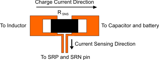
- The charging current-sensing resistor should be placed right next to the inductor output. Route the sense leads connected across the sensing resistor back to the IC in same layer, close to each other (minimize loop area) and do not route the sense leads through a high-current path (see Figure 22 for Kelvin connection for best current accuracy). Place decoupling capacitor on these traces next to the IC
- Place output capacitor next to the sensing resistor output and ground
- Output capacitor ground connections need to be tied to the same copper that connects to the input capacitor ground before connecting to system ground.
- Use a single ground connection to tie charger power ground to charger analog ground; use analog ground copper pour just beneath the IC, but avoid power pins to reduce inductive and capacitive noise coupling.
- Route analog ground separately from power ground. Connect analog ground and connect power ground separately. Connect analog ground and power ground together using power pad as the single ground connection point, or use a 0-Ω resistor to tie analog ground to power ground (power pad should tie to analog ground in this case if possible).
- Decoupling capacitors should be placed next to the IC pins to make trace connection as short as possible.
- It is critical to solder the exposed power pad on the backside of the IC package to the PCB ground. Ensure that there are sufficient thermal vias directly under the IC, connecting to the ground plane on the other layers.
- The via size and number should be enough for a given current path.
See the EVM design for the recommended component placement with trace and via locations. For the QFN information, see SCBA017 and SLUA271.
11.1.1 IC Design Guideline
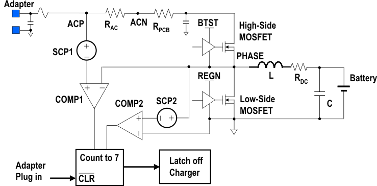
The IC has a unique short circuit protection feature. Its cycle-by-cycle current monitoring feature is achieved through monitoring the voltage drop across Rdson of the MOSFETs after a certain amount of blanking time. In case of MOSFET short or inductor short circuit, the overcurrent condition is sensed by two comparators and two counters will be triggered. After seven times of short circuit events, the charger will be latched off. The way to reset the charger from latch-off status is reconnect adapter. Figure 20 shows the IC short-circuit protection block diagram.
 Figure 20. Block Diagram of IC Short-Circuit Protection
In normal operation, low-side MOSFET current is from source-to-drain, which generates negative voltage drop when it turns on As a result, the overcurrent comparator cannot be triggered. When high-side switch short-circuit or inductor short-circuit happens, the large current of low-side MOSFET is from drain-to-source and can trigger low-side switch overcurrent comparator. IC senses low-side switch voltage drop by PHASE pin and GND pin.
The high-side FET short is detected by monitoring the voltage drop between ACP and PHASE. As a result, it not only monitors the high-side switch voltage drop, but also the adapter sensing resistor voltage drop and PCB trace voltage drop from ACN terminal of RAC to charger high-side switch drain. Usually, there is a long trace between input sensing resistor and charger converting input, a careful layout will minimize the trace effect.
The total voltage drop sensed by IC can be expressed as Equation 15.
where
- RAC is the AC adapter current sensing resistance
- IDPM is the DPM current set point
- RPCB is the PCB trace equivalent resistance
- ICHRGIN is the charger input current
- k is the PCB factor
- RDS(on) is the high-side MOSFET turnon resistance
- IPEAK is the peak current of inductor
Here, the PCB factor k equals 0 means the best layout shown in Figure 24, where the PCB trace only goes through charger input current, while k equals 1 means the worst layout shown in Figure 23, where the PCB trace goes through all the DPM current. The total voltage drop must below the high-side short circuit protection threshold to prevent unintentional charger shutdown in normal operation.
The low-side MOSFET short-circuit voltage drop threshold is fixed to typical 110 mV. The high-side MOSFET short-circuit voltage drop threshold can be adjusted through SMBus command. ChargeOption() bit[8:7] = 00, 01, 10, 11 set the threshold 300 mV, 500 mV, 700 mV, and 900 mV, respectively. For a fixed PCB layout, host should set proper short-circuit protection threshold level to prevent unintentional charger shutdown in normal operation.
11.2 Layout Example
 Figure 21. High-Frequency Current Path
 Figure 22. Sensing Resistor PCB Layout
To prevent unintentional charger shutdown in normal operation, MOSFET RDS(on) selection and PCB layout is very important. Figure 23 shows a PCB layout example that needs improvement and its equivalent circuit. In this layout, system current path and charger input current path are not separated; as a result, the system current causes voltage drop in the PCB copper and is sensed by the IC. The worst layout is when a system current pull-point is after charger input; as a result, all system current voltage drops are counted into overcurrent protection comparator. The worst case for IC is the total system current and charger input current sum equals DPM current. When the system pulls more current, the charger IC tries to regulate RAC current as a constant current by reducing charging current.
 Figure 23. PCB Layout Example: Needs Improvement
Figure 24 shows the optimized PCB layout example. The system current path and charge input current path is separated; as a result, the IC only senses charger input current caused PCB voltage drop and minimized the possibility of unintentional charger shutdown in normal operation. This also makes PCB layout easier for high system current application.
 Figure 24. PCB Layout Example: Optimized