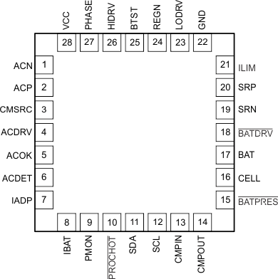
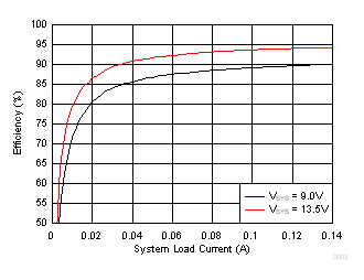
The bq2477x is high-efficiency, synchronous, NVDC-1 battery charge controllers, offering low component count for space-constraint, multi-chemistry battery charging applications.
The power path management allows the system to be regulated at battery voltage but does not drop below system minimum voltage (programmable). With this feature, the system keeps operating even when the battery is completely discharged or removed. The power path management allows the battery to provide supplement current to the system to keep the input supply from being overloaded.
The bq2477x provides drivers and power path management for N-channel ACFET and reverse blocking FET. The devices provides driver to control NVDC operation of external P-channel battery FET. It also drives high-side and low-side MOSFETs of the switching regulator.
The bq2477x monitors adapter current (IADP), battery charge/discharge current (IBAT) and system power (PMON). The flexibly programmed PROCHOT output goes directly to CPU for throttle back when needed.
PART NUMBER | PACKAGE | BODY SIZE (NOM) |
---|---|---|
bq24770 | WQFN (28-Pin) | 4.00mm x 4.00mm2 |
bq24773 |
space
space
Changes from B Revision (October 2014) to C Revision
Changes from A Revision (October 2014) to B Revision
Changes from * Revision (August 2014) to A Revision
bq24770 | bq24773 | |
---|---|---|
Communication Interface | SMBus | I2C |
Communication Address | 0x12H (0x00010010) | D4H (0x11010100) |
Default Switching Frequency | 800kHz | 1.2MHz |
Default Input Current Limit | 3200mA | 2944mA |
Device ID | 0x0114H | 0x41H |
MIN | MAX | UNIT | ||
---|---|---|---|---|
Voltage range | SRN, SRP, ACN, ACP, CMSRC, VCC, BAT, BATDRV | –0.3 | 30 | V |
PHASE | –2.0 | 30 | V | |
BTST, HIDRV, ACDRV | –0.3 | 36 | V | |
LODRV (2% duty cycle) | –4.0 | 7 | V | |
HIDRV (2% duty cycle) | –4.0 | 36 | V | |
PHASE (2% duty cycle) | –4.0 | 30 | V | |
ACDET, SDA, SCL, LODRV, REGN, IADP, IBAT, PMON, BATPRES, ACOK, CELL, CMPIN, CMPOUT, ILIM | –0.3 | 7 | V | |
PROCHOT | –0.3 | 5.5 | V | |
Differential voltage | BTST-PHASE, HIDRV-PHASE | –0.3 | 7 | V |
SRP–SRN, ACP–ACN | –0.5 | 0.5 | V | |
Junction temperature range, TJ | –40 | 155 | °C | |
Storage temperature range, Tstg | –55 | 155 | °C |
MIN | MAX | UNIT | |||
---|---|---|---|---|---|
V(ESD) | Electrostatic discharge | Human body model (HBM), per ANSI/ESDA/JEDEC JS-001, all pins(1) | 0 | 2 | kV |
Charged device model (CDM), per JEDEC specification JESD22-C101, all pins(2) | 0 | 500 | V |
MIN | MAX | UNIT | ||
---|---|---|---|---|
Voltage range | ACN, ACP, CMSRC, VCC | 0 | 24 | V |
BATDRV, BAT, SRN, SRP | 0 | 19.2 | V | |
PHASE | –2 | 24 | V | |
BTST, HIDRV, ACDRV | 0 | 30 | V | |
ACDET, SDA, SCL, LODRV, REGN, IADP, IBAT, PMON, BATPRES, ACOK, CELL, CMPIN, CMPOUT, ILIM | 0 | 6.5 | V | |
PROCHOT | –0.3 | 5.3 | V | |
Differential voltage | BTST-PHASE, HIDRV-PHASE | 0 | 6.5 | V |
SRP–SRN, ACP–ACN | –0.35 | 0.35 | V | |
Junction temperature range, TJ | –20 | 125 | °C | |
Operating free-air temperature range, TA | –40 | 85 | °C |
THERMAL METRIC(1) | bq2477x | UNIT | |
---|---|---|---|
RUY (WQFN) | |||
28 PINS | |||
RθJA | Junction-to-ambient thermal resistance | 33.3 | °C/W |
RθJC(top) | Junction-to-case (top) thermal resistance | 29.7 | °C/W |
RθJB | Junction-to-board thermal resistance | 6.5 | °C/W |
ψJT | Junction-to-top characterization parameter | 0.3 | °C/W |
ψJB | Junction-to-board characterization parameter | 6.5 | °C/W |
RθJC(bot) | Junction-to-case (bottom) thermal resistance | 1.3 | °C/W |
PARAMETER | TEST CONDITION | MIN | TYP | MAX | UNIT | |
---|---|---|---|---|---|---|
OPERATING CONDITIONS | ||||||
V(IN_OP) | Input voltage operating range | 4.5 | 24 | V | ||
MINIMUM SYSTEM VOLTAGE REGULATION (0x3E REGISTER) | ||||||
V(SYSMIN_RNG) | System voltage regulation range | 1.024 | 19.2 | V | ||
V(MINSYS_REG_ACC) | Minimum system voltage regulation accuracy | MinsystemVoltage()=0x2400H | 9.216 | V | ||
–2% | 2% | |||||
MinsystemVoltage()=0x1800H | 6.144 | V | ||||
–3% | 3% | |||||
MinsystemVoltage()=0x0E00H | 3.584 | V | ||||
–3% | 3% | |||||
MAXIMUM SYSTEM VOLTAGE REGULATION (0x15 REGISTER, CHARGE DISABLE) | ||||||
V(SYSMAX_RNG) | System voltage regulation range | 1.024 | 19.2 | V | ||
V(MAXSYS_REG_ACC) | Maximum system voltage regulation accuracy | MaxChargVoltage() = 0x34C0H | 13.504 | V | ||
–2% | 2% | |||||
MaxChargVoltage() = 0x2330H | 9.008 | V | ||||
–3% | 3% | |||||
MaxChargVoltage() = 0x1130H | 4.4 | V | ||||
–3% | 3% | |||||
CHARGE VOLTAGE REGULATION (0x15 REGISTER, CHARGE ENABLE) | ||||||
V(BAT_RGN) | Battery voltage range | 1.024 | 19.2 | V | ||
V(BAT_REG_ACC) | Battery voltage regulation accuranc (0°C - 85°C) | ChargeVoltage() = 0x41A0H | 16.8 | V | ||
–0.5% | 0.5% | |||||
ChargeVoltage() = 0x3130H | 12.592 | V | ||||
–0.5% | 0.5% | |||||
ChargeVoltage() = 0x20D0H | 8.4 | V | ||||
–0.6% | 0.6% | |||||
ChargeVoltage() = 0x1070H | 4.208 | V | ||||
–1% | 1% | |||||
CHARGE CURRENT REGULATION | ||||||
V(IREG_CHG_RNG) | Charge current regulation differential voltage range | V(IREG_CHG) = V(SRP) – V(SRN) | 0 | 81.28 | mV | |
I(CHRG_REG_ACC) | Charge current regulation accuracy 10 Ω current sensing resistor, VBAT > V(SYSMIN) (0°C - 85°C) | ChargeCurrent() = 0x1000H | 4096 | mA | ||
–2% | 2% | |||||
ChargeCurrent() = 0x0800H | 2048 | mA | ||||
–4% | 3% | |||||
ChargeCurrent() = 0x0400H | 1024 | mA | ||||
–6% | 5% | |||||
ChargeCurrent() = 0x0200H | 512 | mA | ||||
–12% | 10% | |||||
I(CLAMP) | Pre-charge current clamp (2s-4s) | CELL = Float or High, BAT below 0x3E(), in LDO mode | 384 | mA | ||
Pre-charge current clamp (1s only) | CELL = LOW, BAT below BATLOWV threshold | 384 | mA | |||
Fast charge current clamp (1s only) | CELL = LOW, BAT above BATLOWV threshold, but below 0x3E() | 2 | A | |||
PRECHARGE CURRENT REGULATION IN LDO MODE | ||||||
I(PRECHRG_REG_ACC) | Precharge current regulation accuracy, VBAT > V(SYSMIN) (0°C - 85°C) | ChargeCurrent() = 0x0180H | 384 | mA | ||
–15% | 15% | |||||
ChargeCurrent() = 0x0100H | 256 | mA | ||||
–20% | 20% | |||||
ChargeCurrent() = 0x00C0H | 192 | mA | ||||
–25% | 25% | |||||
ChargeCurrent() = 0x0080H | 128 | mA | ||||
–30% | 30% | |||||
I(LEAK_SRP_SRN) | SRP, SRN leakage current mismatch | –21 | 21 | µA | ||
LDO MODE TO FAST CHARGE COMPARATOR | ||||||
V(BAT_SYSMIN) | LDO mode to fast charge mode threshold, VBAT rising | as percentage of 0x3E() | 94% | 96% | 99% | |
V(BAT_SYSMIN_HYST) | Fast charge mode to LDO mode threshold hysteresis | as percentage of 0x3E() | 4% | |||
INPUT CURRENT REGULATION | ||||||
V(IREG_DPM_RNG) | Input current regulation differential voltage range | V(IREG_DPM) = V(ACP) – V(ACN) | 0 | 81.28 | mV | |
I(DPM_REG_ACC) | Input current regulation accuracy | ChargeCurrent() = 0x1000H | 4096 | mA | ||
–2 | 2% | |||||
ChargeCurrent() = 0x0800H | 2048 | mA | ||||
–3 | 3% | |||||
ChargeCurrent() = 0x0400H | 1024 | mA | ||||
–5 | 5% | |||||
ChargeCurrent() = 0x0200H | 512 | mA | ||||
–10 | 10% | |||||
I(LEAK_ACP_ ACN) | ACP, ACN leakage current mismatch | ––11 | 20 | µA | ||
INPUT CURRENT SENSE AMPLIFIER | ||||||
V(ACP/N_OP) | Input common mode range | Voltage on ACP/ACN | 4.5 | 24 | V | |
V(IADP_CLAMP) | IADP output clamp voltage | 3.1 | 3.2 | 3.3 | V | |
I(IADP) | IADP output current | 1 | mA | |||
A(IADP) | Input current sense gain | V(IADP)/V(ACP-ACN), ChargeOption0[4]=0, (770/773) | 40 | V/V | ||
V(IADP)/V(ACP-ACN), ChargeOption0[4]=1, (770/773) | 80 | |||||
V(IADP_ACC) | Input current monitor accuracy | V(ACP-ACN) = 40.96 mV | –2% | 2% | ||
V(ACP-ACN) = 20.48 mV | –3% | 4% | ||||
V(ACP-ACN) = 10.24 mV | –6% | 7% | ||||
V(ACP-ACN) = 5.12 mV | –10% | 18% | ||||
C(IADP_MAX) | Maximum output load capacitance | 100 | pF | |||
CHARGE CURRENT AND DISCHARGE CURRENT SENSE AMPLIFIER | ||||||
V(SRP/N_OP) | Battery common mode range | Voltage on SRP/SRN | 2.8 | 18 | V | |
V(IBAT_CLAMP) | IBAT output clamp voltage | 3.1 | 3.2 | 3.3 | V | |
I(IBAT) | IBAT output current | 1 | mA | |||
A(IBAT_DCHG) | Discharge current sensing gain on IBAT pin | V(IBAT)/V(SRN-SRP), ChargeOption0[3]=0 | 8 | V/V | ||
V(IBAT)/V(SRN-SRP), ChargeOption0[3]=1 | 16 | |||||
I(IBAT_DCHG_ACC) | Discharge current monitor accuracy on IBAT pin | V(SRN-SRP) = 40.96 mV | –2% | 2% | ||
V(SRN-SRP) = 20.48 mV | –3% | 3% | ||||
V(SRN-SRP) = 10.24 mV | –5% | 5% | ||||
V(SRN-SRP) = 5.12 mV | –10% | 10% | ||||
A(IBAT_CHG) | Charge current sensing gain on IBAT pin | V(IBAT)/V(SRN-SRP) | 20 | V/V | ||
I(IBAT_CHG_ACC) | Charge current monitor accuracy on IBAT pin (0°C - 85°C) | V(SRN-SRP) = 40.96 mV | –2% | 2% | ||
V(SRN-SRP) = 20.48 mV | –3% | 4% | ||||
V(SRN-SRP) = 10.24 mV | –5% | 7% | ||||
V(SRN-SRP) = 5.12 mV | –10% | 15% | ||||
C(IBAT_MAX) | Maximum output load capacitance | 100 | pF | |||
SYSTEM POWER SENSE AMPLIFIER | ||||||
V(ACP/N_OP) | Input common mode range | Voltage on ACP/ACN | 4.5 | 24 | V | |
V(SRP/N_OP) | Battery common mode range | Voltage on SRP/SRN | 2.8 | 18 | V | |
V(PMON) | Power buffer output voltage | 3.3 | V | |||
V(PMON_CLAMP) | Power buffer clamp voltage | 3 | 3.2 | 3.3 | V | |
I(PMON) | Power buffer output current | 105 | µA | |||
A(PMON) | System power sense gain, V(PMON)/(V(ACP-ACN) x V(ACN) + V(SRN-SRP) x V(SRP)) |
ChargeOption1[9]=0 | 0.25 | µA/V | ||
ChargeOption1[9]=1 | 1 | µA/V | ||||
V(PMON_ACC) | PMON output accuracy | Input 19.5 V, 65W, 1 µA/W | –5% | 5% | ||
Battery 11 V, 44W, 1 µA/W | –6% | 6% | ||||
REGN REGULATOR | ||||||
V(REGN_REG) | REGN Regulator voltage (0 mA - 40 mA) | V(VCC) > 10 V, V(ACDET) > 0.6 V (0 - 50 mA load) | 5 | 5.5 | 6 | V |
V(DROPOUT) | REGN Voltage in drop out mode | V(VCC) = 5 V, I(LOAD) = 20 mA | 4.4 | 4.6 | 4.7 | V |
I(REGN_LIM) | REGN Current Limit when converter is disabled or in T(SHUT) (no charging) | V(REGN) = 4 V, V(ACP) > V(UVLO), 0.6 V < ACDET < 2.4 V | 6.5 | mA | ||
REGN Current Limit when converter is enabled (charging) | V(REGN) = 4 V, V(ACP) > V(UVLO) | 50 | 65 | mA | ||
C(REGN) | REGN Output Capacitor Required for Stability | ILOAD = 100 µA to 50 mA | 1 | µF | ||
QUIESCENT CURRENT | ||||||
I(BAT_BATFET_OFF) | Standby mode. System powered by battery. BATFET off (0°C - 85°C). I(SRN) + I(SRN) + I(SRP)+ I(PHASE) + I(BTST) + I(ACP) + I(ACN) + IBAT + I(CMSRC) + I(VCC) |
VBAT = 16.8 V V(VCC) < V(UVLO), ACDET < 0.6 V |
20 | 27 | µA | |
I(BAT_BATFET_ON) | Standby mode. System powered by battery. BATFET on (0°C - 85°C). I(SRN) + I(SRP) + I(PHASE) + I(BTST) + I(ACP) + I(ACN) + IBAT + I(CMSRC) + I(VCC) |
VBAT = 16.8 V V(VCC) > V(UVLO), ACDET < 0.6 V, 0x12[15]=1, low power mode enabled |
22 | 30 | µA | |
VBAT = 16.8 V V(VCC) > V(UVLO), ACDET < 0.6 V, 0x12[15]=0, 0x3B[2]=0, IBAT Enabled, REGN = 0 |
114 | 150 | µA | |||
VBAT = 16.8 V V(VCC) >V(UVLO), ACDET < 0.6 V, 0x12[15]=0, 0x3B[2]=0, IBAT enabled, REGN = 5.5V |
650 | 775 | µA | |||
I(STANDBY) | Adapter standby quiescent current, I(VCC) + I(ACP) + I(ACN) + I(CMSRC) + I(SRP) + I(SRN) + I(PHASE) + I(BTST) |
ACN = ACP = CMSRC = VCC = 20 V, VBAT = 12.6V, V(ACDET) > 2.4V, CELL pul up, TJ = 0°C - 85°C |
650 | 815 | µA | |
I(AC_SWLIGHT) | Adapter current, I(VCC) + I(ACP) + I(ACN) + I(CMSRC) + I(SRP) + I(SRN) + I(PHASE) + I(BTST) |
I(STANDBY) plus supply current in PFM, 200mW output; Reg0x12[10]=0;MOSFET Qg=4 nF; |
1.5 | 2 | mA | |
I(STANDBY) plus supply current in PFM, 200mW output, Reg0x12[10]=1; limit 40kHz, MOSFET Qg=4 nF; |
3 | 5 | mA | |||
I(AC_SW) | Adapter current, I(VCC) + I(ACP) + I(ACN) + I(CMSRC) + I(SRP) + I(SRN) + I(PHASE) + I(BTST) |
V(ULVO) < V(VCC) < V(ACOVP), VBAT = 16.8 V, V(ACDET) >2.4 V, charge enabled, 800k Hz switching, MOSFET Qg=4 nF |
8 | mA | ||
ACOK COMPARATOR | ||||||
V(ACOK_RISE) | ACOK rising threshold | V(VCC) > V(UVLO), ACDET rising | 2.37 | 2.4 | 2.43 | V |
V(ACOK_FALL) | ACOK falling threshold | V(VCC) > V(UVLO) | 2.32 | 2.35 | 2.38 | V |
V(ACOK_RISE_DEG) | ACOK rising deglitch to turn on ACFET | V(VCC) > V(UVLO) | 2 | ms | ||
V(ACOK_FALL_DEG) | ACOK falling deglitch to turn off ACFET | V(VCC) > V(UVLO) | 2 | µs | ||
V(WAKEUP_RISE) | WAKEUP detect rising threshold | ACDET rising | 0.56 | 0.8 | V | |
V(WAKEUP_FALL) | WAKEUP detect falling threshold | 0.3 | 0.5 | V | ||
UNDER VOLTAGE LOCKOUT COMPARATOR (UVLO) | ||||||
V(UVLOZ) | VCC undervoltage rising threshold | VCC rising | 2.5 | 2.7 | 2.9 | V |
V(UVLO) | VCC undervoltage falling threshold | VCC falling | 2.3 | 2.5 | 2.7 | V |
SLEEP COMPARATOR (VCC_BAT) | ||||||
V(VCC-BAT_FALL) | VCC-BAT falling threshold | Input connected to VCC via schottky diode | –25 | 55 | 135 | mV |
V(VCC-BAT_RISE) | VCC-BAT rising threshold | 174 | 275 | 370 | mV | |
tVCC_BAT_RDEG | VCC to BAT rising deglitch | VCC rising above SRN deglitch to turn on ACDRV | 4 | ms | ||
tVCC_SRN_FDEG | VCC to BATfalling deglitch | VCC falls below SRN deglitch to turn off ACDRV | 100 | µs | ||
INPUT OVERVOLTAGE COMPARATOR (ACOVP) | ||||||
V(ACOV_RISE) | VCC overvoltage rising threshold | VCC rising | 24 | 26 | 28 | V |
V(ACOV_FALL) | VCC overvoltage falling threshold | VCC falling | 22 | 24.5 | 27.5 | V |
V(ACOV_RISE_DEG) | VCC overvoltage rising deglitch | VCC rising to turn off ACDRV | 100 | µs | ||
V(ACOV_FALL_DEG) | VCC overvoltage falling deglitch | VCC falling falling to turn on ACDRV | 3 | ms | ||
INPUT OVERCURRENT COMPARATOR (ACOC) | ||||||
V(ACOC) | ACP to ACN rising threshold, respect to inputcurrent(), peak |
Voltage across input sense resistor rising, Reg0x12[7]=1 | 270% | 300% | 330% | |
V(ACOC_FLOOR) | Measure between ACP and ACN | Set IDPM to min | 44 | 50 | 55 | mV |
V(ACOC_CEILING) | Measure between ACP and ACN | Set IDPM to max | 174 | 180 | 185 | mV |
tRELAX | Falling deglitch time | Relax Time, No Latchoff | 300 | ms | ||
SYSTEM OVERVOLTAGE COMPARATOR (SYS_OVP) | ||||||
V(SYSOVP_RISE) | System Overvoltage rising threshold to turn off ACFET | CELL = Low | 4.9 | 5 | 5.2 | V |
CELL = Float | 11.9 | 12 | 12.3 | V | ||
CELL = High | 18.4 | 18.5 | 19 | V | ||
V(SYSOVP_FALL) | System Overvoltage falling threshold | CELL = Low | 4.6 | 4.7 | 4.9 | V |
CELL = Float | 10.9 | 11.1 | 11.3 | V | ||
CELL = High | 17.4 | 17.7 | 17.9 | V | ||
IOVP | Discharge current when the OVP stop switching was triggered | On SRP and SRN | 19 | mA | ||
tSYSOVP | Deglitch time to latch off ACFET | 25 | µs | |||
BAT OVERVOLTAGE COMPARATOR (BAT_OVP) | ||||||
V(OVP_RISE) | Overvoltage rising threshold as percentage of V(BAT_REG) | BAT rising | 101% | 102% | 103% | |
V(OVP_FALL) | Overvoltage falling threshold as percentage of V(BAT_REG) | BAT falling | 100% | 101% | 102% | |
IOVP | Discharge current during OVP | On SRP and SRN | 19 | mA | ||
tOVP_RISE | Overvoltage rising deglitch to turn off BATDRV to disable charge | 20 | ms | |||
CONVERTER CYCLE-BY-CYCLE COMPARATOR (ILIM_HI) | ||||||
V(OCP_limit) | Converter over current limit (PH-GND) | Reg0x12 [6]=1 | 249 | 290 | 333 | mV |
Reg0x12 [6]=0 | 142 | 170 | 202 | mV | ||
V(OCP_limit_SYSSHORT) | System Short or SRN < 2.5 V | Reg0x12 [6]=1 | 41 | 66 | 87 | mV |
Reg0x12 [6]=0 | 7 | 31 | 53 | mV | ||
CONVERTER CYCLE-BY-CYCLE UNDER-CURRENT COMPARATOR (UCP) | ||||||
V(UCP_FALL) | Charge Undercurrent falling threshold | PH voltage when LSFET is on | –2.8 | 0.4 | mV | |
BATTERY LOWV COMPARATOR | ||||||
V(BATLV_FALL) | BATLOWV falling threshold | CELL = Low | 2.64 | 2.85 | 3.06 | V |
CELL = Float or High | 5.71 | 5.92 | 6.12 | V | ||
V(BATLV_RHYST) | BATLOWV rising threshold | CELL = Low | 2.89 | 3.10 | 3.31 | V |
CELL = Float or High | 5.96 | 6.17 | 6.37 | V | ||
LIGHT LOAD COMPARATOR (LIGHT_LOAD) | ||||||
VLL(FALL) | Light load falling threshold detected on ACP-ACN | 0 | 0.5 | 1.1 | mV | |
VLL(RISE) | Light load rising threshold detected on ACP-ACN | 0.7 | 1.4 | 2.1 | mV | |
THERMAL SHUTDOWN COMPARATOR | ||||||
T(SHUT) | Thermal shutdown rising temperature | Temperature increasing | 155 | °C | ||
T(SHUT_HYS) | Thermal shutdown hysteresis, falling | 20 | °C | |||
tSHUT_RDEG | Thermal shutdown rising deglitch | 100 | µs | |||
tSHUT_FHYS | Thermal shutdown falling deglitch | 10 | ms | |||
VSYS PROCHOT COMPARATOR | ||||||
V(SYS_PRO) | V(SYS) threshold falling threshold | Reg0x3C [7:6]=00 | 5.75 | V | ||
Reg0x3C [7:6]=01 | 5.9 | 6 | 6.15 | V | ||
Reg0x3C [7:6]=10 | 6.25 | V | ||||
Reg0x3C [7:6]=11 | 6.5 | V | ||||
tSYS_PRO_RISE_DEG | V(SYS) Rising Deglitch for throttling | 20 | µs | |||
ICRIT PROCHOT COMPARATOR | ||||||
V(ICRIT_PRO) | IADP rising threshold for throttling above IDPM | Reg0x3C [15:11]=01001 | 145% | 150% | 155% | |
INOM PROCHOT COMPARATOR | ||||||
V(INOM_PRO) | INOM rising threshold as percentage of IDPM | 106% | 110% | 114% | ||
IDCHG PROCHOT COMPARATOR | ||||||
V(IDCHG_PRO) | IDCHG threshold for throttling for IDSCHG of 6 A | Reg0x3D [15:10]=001100 | 6144 | mA | ||
98% | 104% | |||||
INDEPENDENT COMPARATOR | ||||||
V(INDEP_CMP) | Independent comparator threshold | Reg0x3B [7]=1, CMPIN rising | 1.17 | 1.2 | 1.23 | V |
Reg0x3B [7]=0, CMPIN rising | 2.27 | 2.3 | 2.33 | V | ||
V(INDEP_CMP_HYS) | Independent comparator hysteresis | Reg0x3B [6]=0, CMPIN falling | 100 | mV | ||
PWM OSCILLATOR | ||||||
FSW | PWM Switching frequency | Reg0x12 [9:8]=00 | 510 | 600 | 690 | kHz |
Reg0x12 [9:8]=01 | 680 | 800 | 920 | |||
Reg0x12 [9:8]=10 | 850 | 1000 | 1150 | |||
Reg0x12 [9:8]=11 | 1020 | 1200 | 1380 | |||
BATFET GATE DRIVER (BATDRV) | ||||||
V(BATDRV_ON) | Gate Drive Voltage on BATFET | V(SRN) - V(BATDRV) when BAT = 16 V | 8.5 | 9.5 | 10.5 | V |
R(BATDRV_ON) | Measured by sourcing 10 µA current to BATDRV | 3 | 3.5 | 4 | kΩ | |
R(BATDRV_OFF) | Measured by sinking 100 µA current from BATDRV | 1.5 | 2 | 2.5 | kΩ | |
ACFET GATE DRIVER (ACDRV) | ||||||
I(ACFET) | ACDRV charge pump current limit | V(ACDRV) – V(CMSRC)= 5 V | 40 | 60 | µA | |
V(ACDRV_ON) | Gate drive voltage on ACFET | V(ACDRV) – V(CMSRC)when V(VCC) > V(UVLO) | 5.5 | 6.2 | V | |
R(ACDRV_OFF) | ACDRV turn-off resistance | I = 30μA | 5 | 6.2 | 7.4 | kΩ |
R(ACDRV_LOAD) | Minimum load between gate and source | 500 | kΩ | |||
PWM HIGH SIDE DRIVER (HIDRV) | ||||||
RDS(HI_ON) | High side driver(HSD) turn-on resistance | V(BTST) – V(PH) = 5 V | 4 | Ω | ||
RDS(HI_OFF) | High side driver turn-off resistance | V(BTST) – V(PH) = 5 V | 0.65 | 1.3 | Ω | |
V(BTST_REFRESH) | Bootstrap refresh comparator falling threshold voltage | V(BTST) – V(PH) when low side refresh pulse is requested | 3.5 | 3.8 | 4.1 | V |
PWM LOW SIDE DRIVER (LODRV) | ||||||
RDS(LO_ON) | Low side driver (LSD) turn-on resistance | V(BTST) – V(PH) = .55 V | 5.5 | Ω | ||
RDS(LO_OFF) | Low side driver turn-off resistance | V(BTST) – V(PH) = 5.5 V | 1 | 1.45 | Ω | |
INTERNAL SOFT START | ||||||
I(CHG_DAC) | Soft start step size | 64 | mA | |||
Soft start step time | 30 | µs | ||||
INTEGRATED BTST DIODE | ||||||
VF | Forward bias voltage | IF = 20 mA at 25°C | 0.8 | V | ||
VR | Reverse breakdown voltage | IR = 2 µA at 25°C | 20 | V | ||
PWM DRIVERS TIMING | ||||||
tDEADTIME_RISE | Driver dead time from low side to high side | 20 | ns | |||
tDEADTIME_FALL | Driver dead time from high side to low side | 20 | ns | |||
LOGIC INPUT (SDA, SCL) | ||||||
V(IN_ LO) | Input low threshold | I2C (bq24773) | 0.4 | V | ||
SMBus (bq24770) | 0.8 | V | ||||
V(IN_ HI) | Input high threshold | I2C (bq24773) | 1.3 | V | ||
SMBus (bq24770) | 2.1 | V | ||||
LOGIC OUTPUT OPEN DRAIN (ACOK, SDA,CMPOUT) | ||||||
V(OUT_ LO) | Output saturation voltage | 5 mA drain current | 0.4 | V | ||
V(OUT_ LEAK) | Leakage current (ACOK, SDA, SCL) | V = 7 V | –1 | 1 | µA | |
LOGIC OUTPUT OPEN DRAIN (PROCHOT) | ||||||
V(OUT_ LO) | Output saturation voltage | 50 Ω pull up to 1.05 V/ 5mA load | 300 | mV | ||
V(OUT_ LEAK) | Leakage current | V = 5.5 V | –1 | 1 | µA | |
ANALOG INPUT (CELL) | ||||||
V(CELL_HIGH) | 3S/4S | REGN = 5.4 V | 1.9 | V | ||
V(CELL_FLOAT) | 2S | REGN = 5.4 V | 1.2 | 1.8 | V | |
V(CELL_LOW) | 1S | REGN = 5.4 V | 1.1 | V | ||
R(CELL_UP) | Internal resistor between CELL and REGN | 405 | kΩ | |||
R(CELL_DN) | Internal resistor between CELL and GND | 141 | kΩ | |||
ANALOG INPUT (/BATPRES) | ||||||
V(BATPRES_RISE) | BATPRES pin rising threshold | BATPRES rising | 2.1 | 2.2 | 2.3 | V |
V(BATPRES_FALL) | BATPRES pin falling threshold | BATPRES falling | 2 | 2.05 | 2.1 | V |
MIN | TYP | MAX | UNIT | ||
---|---|---|---|---|---|
SMBus TIMING CHARACTERISTICS | |||||
tr | SCLK/SDATA rise time | 1 | µs | ||
tf | SCLK/SDATA fall time | 300 | ns | ||
tW(H) | SCLK pulse width high | 4 | 50 | µs | |
tW(L) | SCLK Pulse Width Low | 4.7 | µs | ||
tSU(STA) | Setup time for START condition | 4.7 | µs | ||
tH(STA) | START condition hold time after which first clock pulse is generated | 4 | µs | ||
tSU(DAT) | Data setup time | 250 | µs | ||
tH(DTA) | Data hold time | 300 | µs | ||
tSU(STOP) | Setup time for STOP condition | 4 | µs | ||
t(BUF) | Bus free time between START and STOP condition | 4.7 | µs | ||
FS(CL) | Clock Frequency | 10 | 100 | KHz | |
HOST COMMUNICATION FAILURE | |||||
ttimeout | SMBus bus release timeout(1) | 25 | 35 | ms | |
tBOOT | Deglitch for watchdog reset signal | 10 | ms | ||
tWDI | Watchdog timeout period, ChargeOption() bit [14:13] = 01(2) | 35 | 44 | 53 | s |
Watchdog timeout period, ChargeOption() bit [14:13] = 10(2) | 70 | 88 | 105 | s | |
Watchdog timeout period, ChargeOption() bit [14:13] = 11(2) (default) | 140 | 175 | 210 | s |
VIN = 12V/5V |
VIN = 12V/5V |
VIN = 19V |
VIN = 19V |