JAJSLQ0 November 2021 BQ25173
PRODUCTION DATA
- 1 特長
- 2 アプリケーション
- 3 概要
- 4 Revision History
- 5 Pin Configuration and Functions
- 6 Specifications
- 7 Detailed Description
- 8 Application and Implementation
- 9 Power Supply Recommendations
- 10Layout
- 11Device and Documentation Support
- 12Mechanical, Packaging, and Orderable Information
5 Pin Configuration and Functions
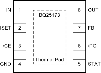
 Figure 5-1 DSG (WSON)
Package
8-Pin
Top View
Figure 5-1 DSG (WSON)
Package
8-Pin
Top ViewTable 5-1 Pin Functions
| PIN | I/O(1) | DESCRIPTION | |
|---|---|---|---|
| NAME | NO. | ||
IN | 1 | P | Input power. Connect to external DC supply. Bypass IN with at least 1-μF capacitor to GND, placed close to the IC. |
ISET | 2 | I | Programs the device fast-charge current, ICHG. External resistor from ISET to GND defines fast-charge current value. Expected range is 30 kΩ (10 mA) to 375 Ω (800 mA). ICHG = KISET / RISET. |
| CE | 3 | I | Active low charge enable pin. Charging is enabled when the CE pin is LOW. IC remains in Shutdown mode and charging is disabled when the CE pin is HIGH. An internal pulldown resistor (RPD_CE) enables the IC by default if this pin is floating. |
| GND | 4 | – | Ground pin. |
| STAT | 5 | O | Open-drain charger status indication output. Connect to pullup rail with a 10-kΩ resistor. LOW indicates VOUT has reached 98% of the programmable regulation voltage, VREG. HIGH indicates charge in progress. |
| PG | 6 | O | Open-drain charger power-good output. Connect to pullup rail with a 10-kΩ resistor. PG goes LOW when VIN > VIN_LOWV and VOUT + VSLEEPZ < VIN < VIN_OV. |
| FB | 7 | I | Programs the supercapacitor regulation voltage, VREG. Use a feedback divider not exceeding 1 MΩ from VOUT to GND to set the regulation voltage. The bottom of the resistor divider network can be connected to PG for reduced power consumption when the input is removed (for VREG ≤ 5 V). |
| OUT | 8 | P | Supercapacitor connection. System load may be connected in parallel with supercapacitor. Bypass OUT with at least 1-μF capacitor to GND, placed close to the IC. |
| Thermal Pad | — | P | Exposed pad beneath the IC for heat dissipation. Solder thermal pad to the board with vias connecting to solid GND plane. |
(1) I = Input, O = Output, P = Power